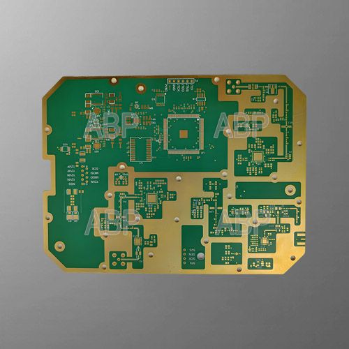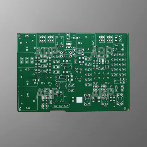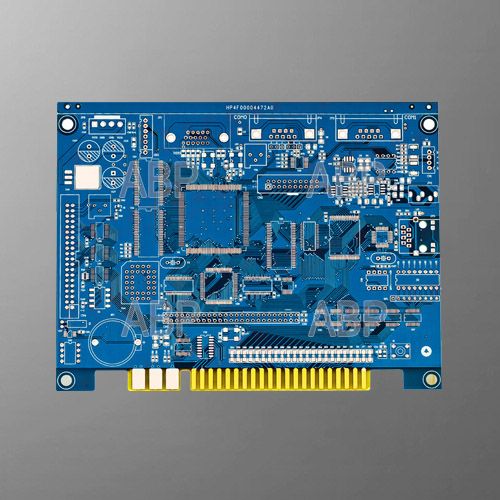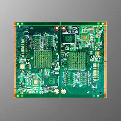
PCB Fabrication
ABP Electronics Founded in Hong Kong in 2004, initially provided global PCB sourcing and trading services to customers around the world. In 2008, we expanded our capabilities by investing in our own advanced PCB manufacturing facility, focusing on high-quality prototype, small-batch, and medium-volume production.
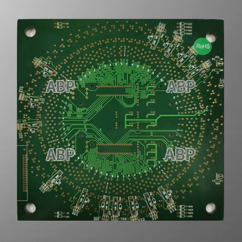
Today, we specialize in manufacturing complex, high-reliability PCBs, including high-layer count boards, high-speed designs, high-precision circuits, and advanced HDI (High-Density Interconnect) boards. Our technical expertise and modern production processes allow us to meet the demanding requirements of today’s advanced electronics applications across industries such as telecommunications, industrial automation, medical, automotive, and consumer electronics.
In addition to superior PCB fabrication, ABP Electronics offers comprehensive component procurement and full PCBA (PCB Assembly) services. This enables us to serve as a true one-stop electronic manufacturing partner — from PCB design support and fabrication to component sourcing, assembly, testing, and finished product integration.
With over 20 years of experience serving international customers, we are committed to delivering exceptional quality, competitive lead times, and reliable supply chain solutions. Our goal is to provide a seamless, efficient, and high-performance one-stop electronics manufacturing platform that helps our customers accelerate product development and achieve long-term success in the global market.
Technical Capabilities
| Item | Capability |
|---|---|
| Layers | 1-30 |
| Thicker Copper | 1-6OZ |
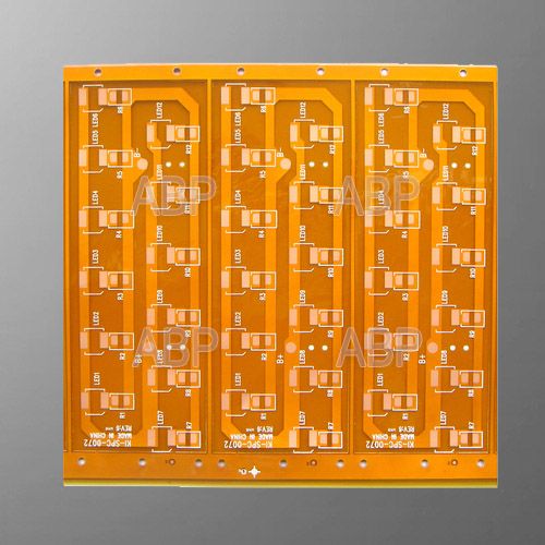
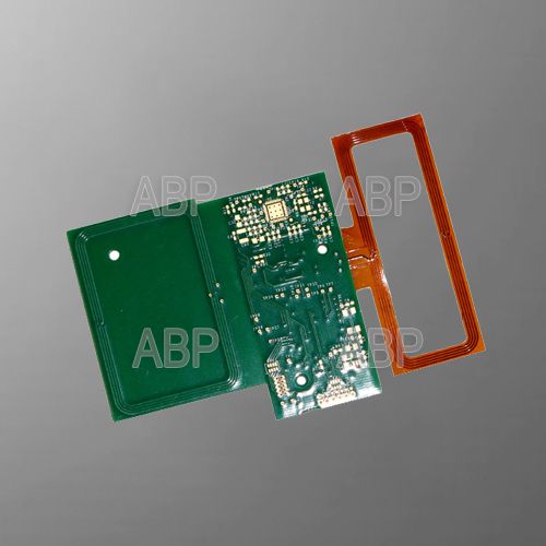
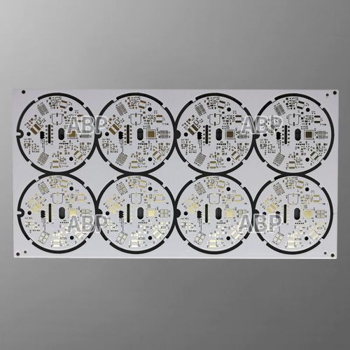
| Products Type | HF(High-Frequency)&(Radio Frequency) board, Impedance controlled board , HDI board ,BGA& Fine Pitch board |
| Solder Mask | Nanya&Taiyo ;LPI & Matt Red, green, yellow,white, blue,black. |
| Base material | FR4(Shengyi China、ITEQ, KB A+,HZ), HI-TG, FR06, Rogers,Taconic、Argon and so on |
| Finished Surface | Conventional HASL,Lead-free HASL,Falsh Gold, ENIG (Immersion Gold)OSP(Entek), Immersion Tin,ImmersionSilver,Hard Gold |
| Selective Surface Treatment | ENIG(immersion Gold)+OSP, ENIG(immersion Gold)+Gold Finger,Flash Gold +Gold Finger,immersion Silver+ Gold Finger, Immersion Tin+Gold Finger |
| Technical Specification | Minimum line width/gap:3.5/4mil(laser drill) Minimum hole size:0.15mm(mechanical drill)/4mil(laser drill) Minimum Annular Ring: 4mil Max Copper thickness: 6OZ Max Production size:900×1200mm Board Thickness:D/S: 0.2-7.0mm, Multilayers:0.40-7.0mm, Min Solder Mask Bridge:0.08mm Aspect ratio: 15:1 Plugging Visa capability: 0.2-0.8mm |
| Tolerance | Plated holes Tolerance:0.08mm(min±0.05) Non-plated hole tolerance:0.05min(min+0/-0.05mm or +0.05/-0mm) Outline Tolerance:0.15min(min±0.10mm) Functional test : Insulating resistance : 50 ohms (mormality) Peel off strength: 1.4N/mm Thermal Stress test :2650c,20 seconds Solder mask hardness:6H E-Test voltage :500V+15/-0V 30S Warp and Twist: 0.7% (semiconductor test board≤0.3% ) |
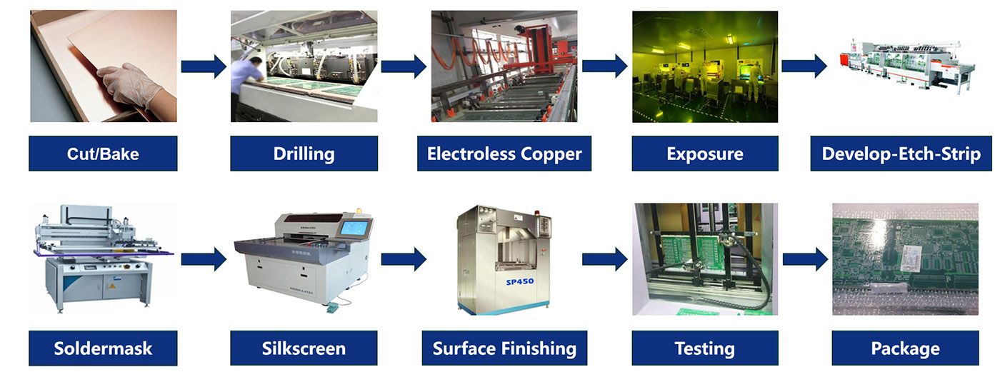
Production Control Process
Product Display