Starting a project without first counting the cost can end up being an expensive mistake, and this principle doesn’t apply to only large construction projects. Any project should be evaluated first for its cost to avoid unpleasant surprises, and this includes getting a printed circuit board manufactured.
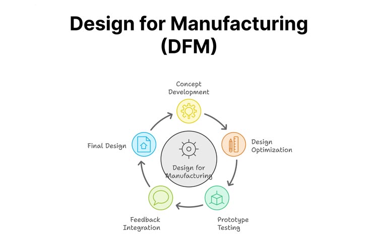
There are design for manufacturing (DFM) rules that must be followed during PCB layout to ensure that the design is optimized for manufacturing, and if those rules are not followed it could result in expensive consequences. To make sure that your board’s layout is optimized for the most efficient manufacturing, you should conduct a cost effectiveness analysis before you send it off to be built. Here are some ideas that can help.

What to Look for in Your Layout for a Cost Effectiveness Analysis
The goal that you are trying to achieve is to design your printed circuit board so that it can be manufactured without any problems. You may have some really new and innovative ideas, but it won’t do you any good if the board can’t built. By analyzing the design from a manufacturability cost effectiveness perspective during layout, you can avoid potential assembly problems. Here are some of the areas that you should focus on:
-Bill of Materials (BOM): Any errors in the BOM may result in the wrong parts being purchased, stocked, and prepped for assembly. If these errors are not found in time, it may even result in the wrong parts being assembled on the board.
-Component Clearance: Parts that do not have enough clearance between each other or other board features cause problems for assembly, test, and re-work.
-Component Placement & Rotation: Parts that are too close to each other or are rotated incorrectly can cause shadowing during wave soldering. This can result in improper solder fillets being formed leading to bad solder connections.
-Footprint Land Pattern Sizes: Footprint pad sizes that are too small or incorrectly placed can also lead to poor solder joints, while pads that are too large can cause parts to miss-align during solder reflow.
-Solder Mask Coverage: Solder may bridge between footprint pads if they do not have adequate solder mask coverage between them. This bridging can result in unintentional shorts between the pads.
-Testability Coverage: The manufacturer will run a completed circuit board through test to validate its assembly. If adequate test point coverage is not provided for in the design, the manufacturer will have to resort to other more expensive options.
All of these areas may end up passing the minimum design rules that you have set up for your layout, but they may not be the most optimum conditions for manufacturability. By taking the time to look at these areas from a manufacturing cost effectiveness perspective, it can help you to make subtle alterations to your layout which will yield much better results at the assembly house. Next we’ll look at some of the extended consequences that these manufacturing problems can cause.
How These Layout Errors Translate to Manufacturing Problems
As we saw above, there are many issues in the design that may seem minor during layout, but can add up to significant and expensive problems for manufacturing. Here are some of the worse case results from those same problems:
-Incorrect Parts in the BOM: Your circuit board goes through an extensive process during manufacturing that starts with the purchasing of the parts. If the wrong components have been specified in the BOM, then the wrong components may end up being purchased, stocked, and loaded into pick and place machines for assembly. This in itself can be a costly problem, but it gets worse if these parts are assembled on the board. Now you will incur the cost of manual rework to correct the problem. Even worse, parts that are marginally incorrect(such as an incorrect tolerance value)may work initially, but fail later in the field causing even more expense in debug and repair.
-Insufficient Component Clearance: When components are too close to each other, it may interfere with automated assembly techniques. Having to manually assemble and test parts or even rework tight areas of the board will add additional and unexpected expenses.
-Bad Solder Joints: Bad solder connections are prone to breaking if they haven’t already done so during assembly. These breaks may cause outright part failures, which will result in extra time to test, find, and repair the bad connections. Even worse though are the intermittent failures which are difficult to locate and correct. Problems like this can become very costly in a short amount of time.
-Solder Reflow Problems: An abundance of solder due to oversized pads may result in surface mount parts floating out of position. These parts may now be too close to other parts causing potential clearance or even shorting problems. Unbalanced solder reflow on smaller parts due to differing pad sizes, may result in those pats standing on end during solder reflow in an effect called “tombstoning”. Once again, this will require more rework to repair.
Solder Slivers: Solder bridging between pads without adequate solder mask coverage will require manual rework to remove. Some of these silvers can be very small and difficult to find adding to the time and expense for repair.
Incomplete Test Coverage: To validate the assembly of a board that doesn’t have adequate teat coverage, the manufacturer will have to resort to other more costly test methods. Manual bench tests are slow and expensive for large boards with thousands of connections, and not as reliable as automated test procedures.
As you can see, the more these errors are allowed to accumulate, the most potential manufacturing delay and cost may add up. The best thing to do is to evaluate your design for its manufacturability cost effectiveness from the start, and design out any potential problems before you send it out for fabrication and assembly.
