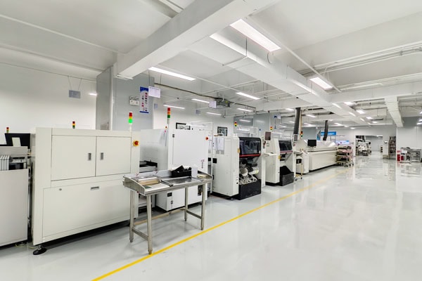
In the journey of an electronic product from concept to market, the leap from design to mass production is the most critical phase. Many projects encounter bottlenecks at this stage—cost overruns, schedule delays, and low product yields—often not due to manufacturing erroes, but rather tracing back to the source: the PCB design. A well-designed PCB is like laying a solid foundation for a building; it not only determines the product’s performace and reliability but also heavily influences the difficulty and cost of subsequent SMT (Surface Mount Technology) assembly. In short, PCB design is the “DNA” of the entire electronics manufacturing chain. Good design DNA gives rise to an efficient, low-cost production process.
1.Optimizing Design for Manufacturabiliey: From “Producible” to “Easily Producible”
Design for Manufacturability (DFM) is the bridge that connects design and manufacturing. A PCB design that ignores DFM may be functionally powerful but can turn into a nightmare on the assembly floor. A good design is first reflected in a deep understanding of and respect for the SMT process.
1.1 Rational Component Layout and Spacing:
SMT placement machines have limited precision in their pick-and-place operations. If components are placed too densely or with insufficient spacing, two serious problems arise: first, the machine may cause “component collisions” during placement, damaging expensive components and nozzles; second, it makes rework and manual soldering nearly impossible. A good design follows the recommended spacing guidelines provided by the SMT factory, ensuring adequate clearance between components. This not only improves production efficiency but also greatly reduces the risk of damage and rework.
1.2 Standardized Pad Design and Solder Mask Control:
Each component has specific pad size and shape requirements. Incorrectly sized pads can lead to soldering defects such as “tombstoning” (where one end of a component lifts off the pad), “offset,” or “insufficient solder.” Additionally, improper solder mask openings can cause solder bridging between adjacent pads. A good design strictly follows IPC standards or component manufacturer recommendations for pad design and ensures precise alignment between the solder mask layer and the copper layer. This seemingly small detail directly impacts soldering quality and first-pass yield, significantly reducing the need for rework and lowering overall costs.
2. Simplifying the Production Process: Reducing Steps Means Lowering Costs
A complex production process inevitably leads to higher costs. A thoughtful PCB design can simplify the SMT assembly flow, reducing the number of production steps and associated risks.
2.1 Minimizing the Need for Manual Soldering and Rework:
While SMT is highly automated, certain special components (such as large connectors, transformers, or some heat-generating ICs) may still require manual soldering or wave soldering. A good design minimizes the use of such components or cleverly designs their placement and orientation to make them compatible with standard SMT processes. For example, using SMT-compatible connectors instead of through-hole ones can eliminate an entire wave soldering process, significantly shortening the production cycle and reducing labor and material costs.
2.2 Optimizing Panelization for Mass Production:
In mass production, PCBs are often assembled in panels to maximize machine utilization. A poorly designed panel can result in low material utilization, difficult de-paneling, or even damage to components near the edges. A good design considers panel layout from the early stages, including optimizing the arrangement of individual boards, adding appropriate tooling holes and fiducial marks, and using robust de-paneling methods like V-scoring or tab routing. This not only improves production efficiency but also reduces material waste and the risk of damage during handling.
3. Improving Product Yield: The Most Direct Way to Lower Costs
Yield is one of the most critical metrics in manufacturing. Even a small increase in yield can lead to significant cost savings. PCB design plays a decisive role in achieving high yields.
3.1 Ensuring Heat Distribution and Welding Reliability:
Components with high power consumption or large thermal masses (e.g., CPUs, power converters) can cause uneven heat distribution during reflow soldering, leading to cold solder joints or virtual soldering. A good design uses “thermal relief pads” or “spoke” connections to isolate large copper areas from component pads, ensuring even heat transfer. This allows each solder joint to form a reliable intermetallic compound under the ideal temperature profile, fundamentally preventing welding defects.
3.2 Enhancing Testability and Debugging Convenience:
Design must leave “doors” for production testing and later debugging. Adequate test point placement facilitates fast and comprehensive inspection using ICT (In-Circuit Test) or FCT (Functional Test) fixtures, enabling early detection and isolation of issues during production. Without reserved test points or with difficult-to-access points, testing efficiency plummets, potentially requiring manual point-by-point troubleshooting—a process that exponentially increases both cost and time.
In summary, PCB design is far more than just the physical implementation of a schematic; it is a comprehensive art that integrates electronic engineering, materials science, thermodynamics, and manufacturing processes. A good PCB design proactively reduces manufacturing difficulty and cost at the source by optimizing DFM, simplifying workflows, and improving product yield. It eliminates potential manufacturing problems on the drawing board and maximizes production line efficiency. Therefore, for any electronic product project aiming for successful mass production, investing in meticulous PCB design is not an optional expense—it is the highest-return strategic investment.

