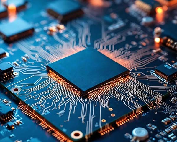
In the era of miniaturization, where smartphones are thinner than a coin and wearable devices fit seamlessly on the skin, the demand for smaller, faster, and more powerful electronics has never been greater. At the heart of this technological revolution lies the High-Density Interconnect (HDI) printed circuit board (PCB)—a marvel of engineering that has become the core component enabling the next generation of electronic devices. By packing more functionality into less space, HDI PCBs are not just supporting innovation; they are driving it.

What Are HDI PCBs?
HDI PCBs are advanced circuit boards characterized by their high wiring density, which includes microvias (vias with diameters less than 150 micrometers), fine lines (trace widths and spaces as small as 75 micrometers or less), and multiple layers interconnected through blind and buried vias. Unlike traditional PCBs, which rely on larger through-holes and wider traces, HDI technology optimizes space by stacking layers vertically and using microstructures to route signals. This allows for a significant increase in component density without expanding the board’s footprint.
Enabling Miniaturization and Performance
The primary advantage of HDI PCBs is their ability to support miniaturization without compromising performance. Modern devices like smartphones, tablets, and medical implants require complex circuitry to handle high-speed data processing, 5G connectivity, and advanced sensors. HDI PCBs meet these demands by:
- Reducing Size and Weight: By eliminating bulky through-holes and using microvias, HDI boards can be up to 70% smaller and lighter than traditional PCBs. This is critical for wearables, drones, and aerospace applications where every gram matters.
- Improving Electrical Performance: Shorter signal paths and reduced via stubs minimize signal loss and electromagnetic interference (EMI), ensuring faster data transmission and higher reliability. This is essential for high-frequency applications like 5G antennas and artificial intelligence (AI) processors.
- Enhancing Thermal Management: HDI PCBs often incorporate thermal vias and copper-in-plated holes to dissipate heat more efficiently, preventing overheating in compact, high-power devices like electric vehicle (EV) control units.
Powering Key Technological Trends
HDI PCBs are the backbone of several transformative technologies shaping the future:
- 5G and IoT: The Internet of Things (IoT) relies on billions of interconnected devices, many of which are small and battery-powered. HDI PCBs enable the compact, low-power designs needed for smart sensors, connected home devices, and industrial IoT modules.
- Automotive Electronics: Modern EVs contain over 100 electronic control units (ECUs) for functions like autonomous driving, battery management, and infotainment. HDI PCBs provide the high-density, high-reliability interconnects required for these systems, where failure is not an option.
- Medical Devices: From implantable pacemakers to handheld diagnostic tools, medical electronics demand extreme miniaturization and biocompatibility. HDI PCBs allow for complex circuitry in tiny form factors, enabling life-saving innovations.
Challenges and Future Directions
Despite their benefits, HDI PCBs present unique challenges. Manufacturing requires precision equipment for laser drilling microvias, plating fine traces, and aligning multiple layers, driving up production costs. Additionally, design complexity demands advanced simulation tools to ensure signal integrity and thermal performance.
Looking ahead, the future of HDI PCBs lies in further innovation. Researchers are exploring “substrate-like PCBs” (SLPs) with even finer lines (50 micrometers or less) and embedded components to push density limits. Flexible and rigid-flex HDI boards are also gaining traction for applications like foldable phones and wearable sensors, where flexibility is key.
Conclusion
As electronic devices become smaller, smarter, and more integrated, HDI PCBs will remain the core component enabling this evolution. By balancing miniaturization, performance, and reliability, they are not just supporting the future of technology—they are defining it. From 5G networks to autonomous vehicles and medical breakthroughs, HDI PCBs are the unsung heroes powering the innovations that will shape our world. In the electronics industry, the future is high-density, and HDI PCBs are leading the way.
