What is Design For Manufacturing (DFM)?
Design for Manufacturing or Design for Manufacturability (DFM) is the optimisation of a part, product, or component’s design, to create it cheaper and more easily. DFM involves efficiently designing or engineering an object, generally during the product design stage, when it is easier and less expensive to do so, to reduce manufacturing costs. This allows a manufacturer to identify and prevent mistakes or discrepancies.
Principles of DFM
DFM occurs early in product development, before tooling and the assembly process, when the product is being designed. Doing so will make manufacture less time-consuming, which will reduce cost and increase ease of manufacturing. The exact process of DFM will depend on what product is being designed and produced. General principles of DFM include designing objects for efficient assembly, the standardisation of materials and components, reducing the number of parts, and minimising the amount of manufacturing operations required on parts during assembly. Other basics of effective DFM include standardisation of parts to save on part cost, design simplicity, which may reduce the complication or number of parts required, and setup time reduction.
Advantages/Benefits
Products made with DFM will have a lower production cost
Quicker time-to-market
Shortening of the product development process
Production will be up to speed sooner
Parts may be combined to reduce assembly steps and quantity of parts
Catches and removes mistakes or faults
Higher quality of a product, as design can be refined and enhanced at every stage
As construction activities can be removed from a site and placed elsewhere, DFM can create a safer working environment
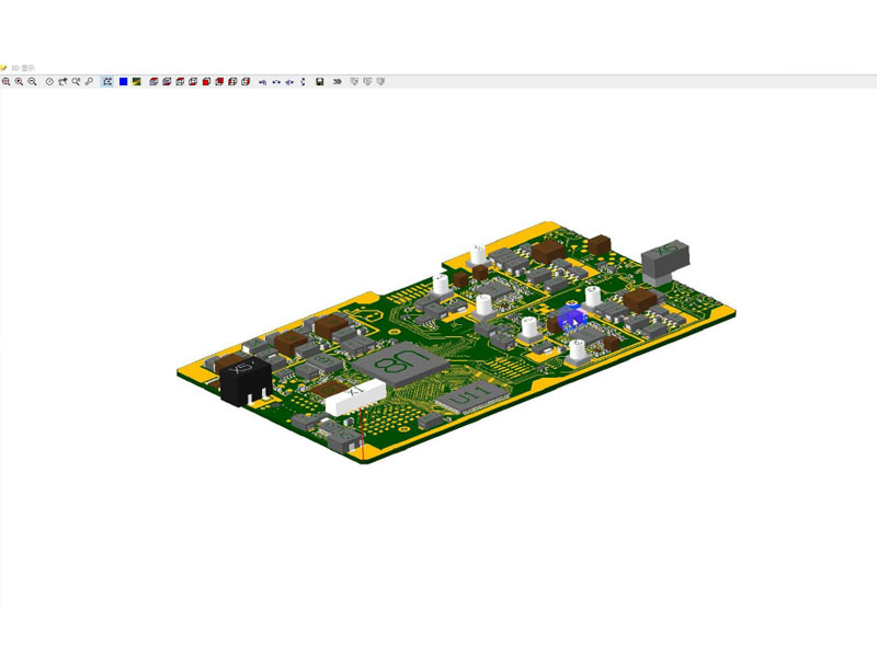
PCB circuit board processing DFM checklist
Clear component number and silk screen
BOM containing manufacturer’s brand and part number, description, tag number
Confirm PCB manufacturing process: material, board thickness, copper thickness, number of layers, surface treatment, character color and special process
Reasonable PCB layer and panel method
Provide the correct SMT patch file
Perfect program burning and functional testing program
Clear finished product assembly manual and schematic diagram
Other special process requirements
Fitting detection of BOM materials and PCB pads (customer engineers often cause the BOM not to be updated in time during the design change process, resulting in the purchase of wrong materials)
DFM analysis reports will be provided