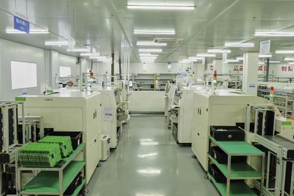
In Surface Mount Technology (SMT) assembly, solder paste printing is often overlooked as a “simple” step, yet it is arguably the most critical process determining final product quality. As the “first line of defense,” solder paste printing sets the foundation for every subsequent stage—component placement, reflow soldering, and inspection. A defect in this initial phase can cascade into costly rework, reduced reliability, or even product failure. This article explores why solder paste printing is pivotal to SMT quality and how its precision directly impacts manufacturing efficiency.

1. The Foundation of Solder Joint Formation
Solder paste—a mixture of solder alloy particles, flux, and solvents—acts as the adhesive and electrical conduit between components and PCB pads. During printing, the paste is deposited through a stencil onto the PCB, forming tiny deposits that must be uniform in volume, shape, and position. These deposits determine how well components align during placement and how solder joints melt and flow during reflow.
If printing is inconsistent—e.g., insufficient paste, misaligned deposits, or smearing—subsequent processes cannot compensate. Insufficient paste leads to weak or open joints, while excess paste causes solder bridging (short circuits). Misaligned deposits force components to shift during placement, resulting in tombstoning or offset solder joints. In short, the quality of solder paste printing is the “gatekeeper” of reliable solder joints.
2. Printing Defects: The Root Cause of Most SMT Failures
Studies show that up to 70% of SMT defects originate from solder paste printing, far exceeding errors from component placement or reflow soldering. Common printing defects include:
- Insufficient or Excessive Paste: Caused by stencil aperture errors, improper squeegee pressure, or paste viscosity issues. Insufficient paste leads to dry joints, while excess paste triggers bridging.
- Misregistration: Occurs when stencil apertures do not align with PCB pads, often due to poor stencil-to-board alignment or mechanical vibration. This results in components being placed on partial or no paste, causing open circuits.
- Smearing or Bleeding: Happens when paste spreads beyond apertures due to high viscosity, low squeegee speed, or damaged stencils. Smearing creates short circuits and complicates inspection.
These defects are difficult to correct later. For example, a misprinted pad cannot be fixed during reflow, and bridging often requires manual rework—a time-consuming, error-prone process.
3. The Economics of Printing Precision
Beyond quality, solder paste printing directly impacts manufacturing costs. A single printing defect can lead to:
- Rework Costs: Manual correction of defects like bridging or insufficient paste increases labor time and delays production.
- Scrap Rates: Severe defects, such as widespread misregistration, may render entire boards unusable, wasting materials and time.
- Equipment Downtime: Troubleshooting printing issues (e.g., adjusting stencil alignment or cleaning stencils) halts production lines, reducing throughput.
Conversely, a well-optimized printing process minimizes these costs. For instance, using laser-cut stencils with nano-coatings reduces paste sticking, ensuring consistent deposits and lowering defect rates by up to 50%.
4. Key Factors for Printing Success
To uphold its role as the “first line of defense,” solder paste printing must be controlled through:
- Stencil Design: Aperture size, shape, and thickness must match PCB pad geometry and component requirements. IPC-7525 standards provide guidelines for optimal stencil design.
- Paste Management: Proper storage (e.g., refrigeration at 5–10°C), thawing, and mixing ensure consistent viscosity. Expired or contaminated paste should never be used.
- Process Parameters: Squeegee pressure, speed, and angle must be calibrated to avoid smearing or insufficient deposition. Modern printers use automated vision systems to verify alignment and deposit volume in real time.
5. The Ripple Effect on Downstream Processes
A well-printed PCB streamlines every subsequent SMT stage. During component placement, accurate paste deposits ensure components self-align due to surface tension forces, reducing placement errors. In reflow soldering, uniform paste volume promotes even heat distribution, minimizing defects like tombstoning or cold joints. Finally, inspection (AOI or X-ray) becomes faster and more reliable, as there are fewer defects to detect.
Solder paste printing is far more than a preliminary step—it is the cornerstone of SMT quality. By ensuring precise, consistent paste deposition, it prevents defects, reduces costs, and sets the stage for efficient downstream processes. As electronics become smaller and more complex, the margin for error narrows, making printing precision even more critical. In the pursuit of high-quality, cost-effective manufacturing, solder paste printing truly stands as the “first line of defense”—a process that, when mastered, defines the success of the entire SMT assembly.
