Many users of PCBs find ceramic PCBs have an advantage over traditional PCBs made of other materials. This advantage is because ceramic PCBs provide suitable substrates for electronic circuits with high thermal conductivity and low coefficient of thermal expansion (CTE).
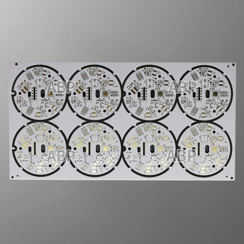
The ceramic PCB is extremely versatile and can replace a complete traditional PCB with a less complex design and increased performance. You can use them in multiple products, like high-power circuits, chip-on-board modules and proximity sensors.
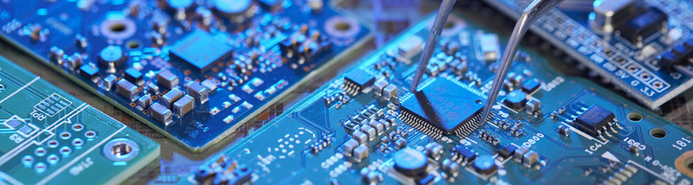
Main Ceramic PCB Types
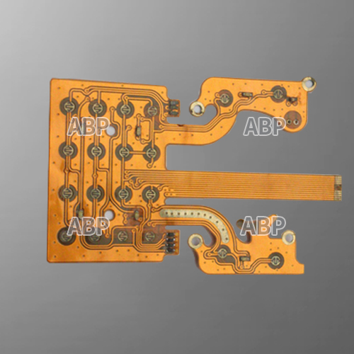
From the level of substrates, ceramic PCBs include the aluminum, AIN, BeO, Si₃N₄, hybrid substrate boards, etc. From the layers of the circuit boards, there are the single-layer, double-layer, and multilayer.
Ceramic PCBs are usually made up of ceramic cores, with alumina and aluminum nitride (AIN) being two of the primary types. Both of these kinds of boards provide better thermal performance than metal core PCBs because there isn’t a need for an electric layer between the core and the circuits. Find out more about these two main kinds of ceramic PCB types below:
AIN: For high thermal conductivity, aluminum nitride boards are ideal, providing greater than 150 w/mK. AIN is a top choice for may other reasons as well, such as its good dielectric properties, non-reactiveness with various semiconductor process chemicals and low CTE.
Alumina: Since aluminum nitride board are expensive, those opting for less expensive ceramic PCBs may find themselves with Alumina boards. These PCBs are made out of aluminum oxide and offer about 18-36 w/mK.
Advantages of Ceramic PCB
Safe operation in temperatures up to 350 degrees Celsius
Simple implementation of high-density circuit tracing
Exceptional high-frequency performance
Versatile packaging, with an option to come in hermetic packages to prevent water absorption
Tough chemical erosion resistance
Another ceramic PCB advantage is a lower overall system cost, which can be especially cost-effective for dense packages, since you have parallel processing of layers.
| Item | Capability |
|---|---|
| Layers | 1-30 |
| Thicker Copper | 1-6OZ |
| Products Type | HF(High-Frequency)&(Radio Frequency) board, Impedance controlled board , HDI board ,
BGA& Fine Pitch board |
| Solder Mask | Nanya&Taiyo ;LPI & Matt Red, green, yellow,white, blue,black. |
| Base material | FR4(Shengyi China、ITEQ, KB A+,HZ), HI-TG, FR06, Rogers,Taconic、Argon and so on |
| Finished Surface | Conventional HASL,Lead-free HASL,Falsh Gold, ENIG (Immersion Gold)OSP(Entek), Immersion Tin,ImmersionSilver,Hard Gold |
| Selective Surface Treatment | ENIG(immersion Gold)+OSP, ENIG(immersion Gold)+Gold Finger,Flash Gold +Gold Finger,
immersion Silver+ Gold Finger, Immersion Tin+Gold Finger |
| Technical Specification | Minimum line width/gap:3.5/4mil(laser drill) Minimum hole size:0.15mm(mechanical drill)/4mil(laser drill) Minimum Annular Ring: 4mil Max Copper thickness: 6OZ Max Production size:900×1200mm Board Thickness:D/S: 0.2-7.0mm, Multilayers:0.40-7.0mm, Min Solder Mask Bridge:0.08mm Aspect ratio: 15:1 Plugging Visa capability: 0.2-0.8mm |
| Tolerance | Plated holes Tolerance:0.08mm(min±0.05) Non-plated hole tolerance:0.05min(min+0/-0.05mm or +0.05/-0mm) Outline Tolerance:0.15min(min±0.10mm) Functional test : Insulating resistance : 50 ohms (mormality) Peel off strength: 1.4N/mm Thermal Stress test :2650c,20 seconds Solder mask hardness:6H E-Test voltage :500V+15/-0V 30S Warp and Twist: 0.7% (semiconductor test board≤0.3% ) |