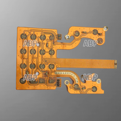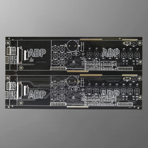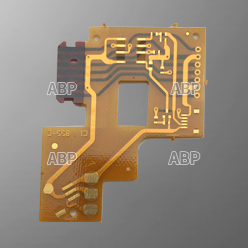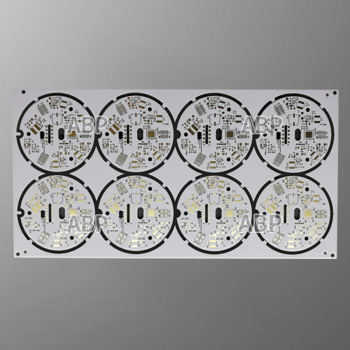
Double sided PCB is popular Type of PCB or Printed Circuit Board. It is little complex than Single Sided PCBs. These types of PCB have one single layer of the base substrate but conductive (copper) layer on both sides of the substrate. Solder mask is applied on both sides of the board.
Holes for electronic components have to be plated through for conductivity on both the circuits. Conductive holes in the PCB allow circuits on one side to attach to circuits on the other side. Electronic components are soldered on both sides. Since, there are two or double conductive layer forming the circuit. It is called double Sided PCB or two layer PCB.
How to Make Double Sided PCB?
It is simple to make double sided PCBs. Following are the steps:
1. Make Top and Bottom Layout of the PCB using any PCB designing software / CAD Tool.
2. Print both the layouts on separate good quality glossy paper.
3. Take a Double Sided Copper plated fiberglass PCB substrate and cut to required size / dimension.
4. With a Cloth Iron (Max Temperature), Iron the Top PCB layout Print on the Top side of the board. This may take 20-30 Seconds.
5. Remove the iron and remove the laser ink from the PCB tracks with a scrubber.
6. Drill the required components holes.
7. Now clean the other side of the board.
8. Repeat Steps 4 to 5 to print the bottom layout of the PCB. Make sure that the layouts of both sides are aligned properly.
9. Place the board in copper chloride solution for about 20-30 minutes so that copper etches out.
10. To make the holes conductive or plated through hole, use conductive ink or conductive pen with fine tip.
11. Apply solder mask on both sides of the board.
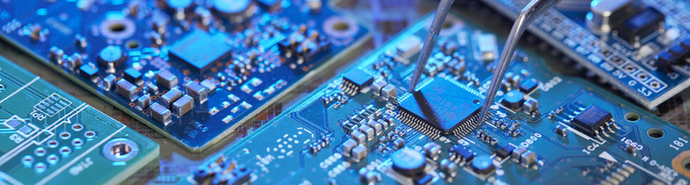
12. Do soldering of all the electronic components.
13. Your Double sided PCBA is ready!
Benefits of Double Sided PCB
Double Sided printed circuit boards offer following benefits:
1. Provides more flexibility.
2. Increased circuit density.
3. Reduced board size.
4. Optimum use of available space as there is space for components on both sides of the board.
5. Can be used in numerous electronic devices.
6. More complicated projects can be designed.
7. Cost effective.
Application of Double Sided PCB
Double Sided Printed Circuit Boards offer more flexibility and increased circuit density. This is why many electronic companies in the world use these boards in several electronic devices.
-Converters and UPS power system
-Control relays and power conversion
-HVAC and LED lighting
-Instrumentation and industrial controls
-Power supplies and regulators
-Traffic control system
-Vending machines
-Line reactors, test and monitoring equipment
-Automotive dashboards
| Item | Capability |
|---|---|
| Layers | 1-30 |
| Thicker Copper | 1-6OZ |
| Products Type | HF(High-Frequency)&(Radio Frequency) board, Impedance controlled board , HDI board ,
BGA& Fine Pitch board |
| Solder Mask | Nanya&Taiyo ;LPI & Matt Red, green, yellow,white, blue,black. |
| Base material | FR4(Shengyi China、ITEQ, KB A+,HZ), HI-TG, FR06, Rogers,Taconic、Argon and so on |
| Finished Surface | Conventional HASL,Lead-free HASL,Falsh Gold, ENIG (Immersion Gold)OSP(Entek), Immersion Tin,ImmersionSilver,Hard Gold |
| Selective Surface Treatment | ENIG(immersion Gold)+OSP, ENIG(immersion Gold)+Gold Finger,Flash Gold +Gold Finger,
immersion Silver+ Gold Finger, Immersion Tin+Gold Finger |
| Technical Specification | Minimum line width/gap:3.5/4mil(laser drill) Minimum hole size:0.15mm(mechanical drill)/4mil(laser drill) Minimum Annular Ring: 4mil Max Copper thickness: 6OZ Max Production size:900×1200mm Board Thickness:D/S: 0.2-7.0mm, Multilayers:0.40-7.0mm, Min Solder Mask Bridge:0.08mm Aspect ratio: 15:1 Plugging Visa capability: 0.2-0.8mm |
| Tolerance | Plated holes Tolerance:0.08mm(min±0.05) Non-plated hole tolerance:0.05min(min+0/-0.05mm or +0.05/-0mm) Outline Tolerance:0.15min(min±0.10mm) Functional test : Insulating resistance : 50 ohms (mormality) Peel off strength: 1.4N/mm Thermal Stress test :2650c,20 seconds Solder mask hardness:6H E-Test voltage :500V+15/-0V 30S Warp and Twist: 0.7% (semiconductor test board≤0.3% ) |