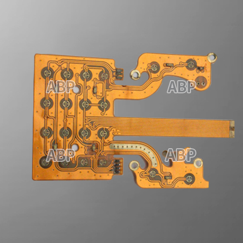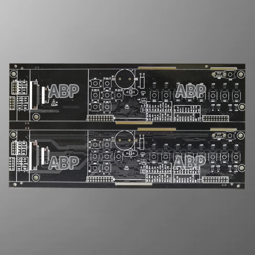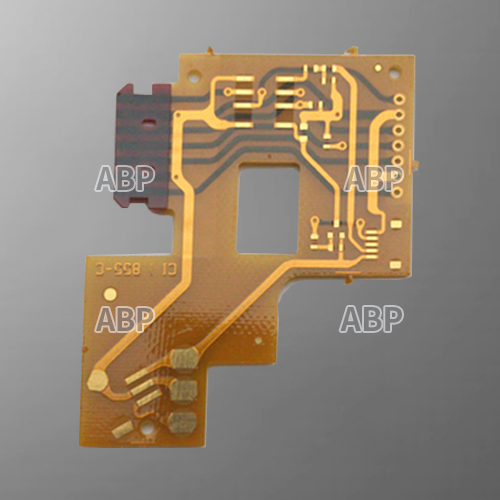
What are HDI PCBs?
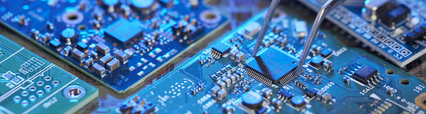
High Density Interconnect (HDI) printed circuit boards (PCBs) are defined as PCBs with higher wiring density per unit area than conventional PCBs. Nowadays, HDI PCBs are increasingly being used, and have made a big difference to technological advancement in electronics industry.
What are the benefits of HDI PCB?
HDI PCBs have many benefits for users over traditionally manufactured circuit boards. There are some benefits:
1. Excellent Versatility: High density interconnect circuit boards are typically used in applications in which weight, space, reliability, and performance are major concerns. Thus, HDI circuit boards are used in a wide range of applications that are related to aeronautics, consumer products, electronics, and computers.
2. Compact Designs: With HDI boards, you can secure more components on both sides of the raw PCB, allowing you to get more functionality out of a smaller space and expanding the overall capabilities of the equipment. HDI technology enables you to add functionality while reducing the size and weight of your products.
3. Improved Reliability: The smaller aspects ratios and the high-quality construction of microvias can increase the reliability of your board and your product. The improved performance and reliability HDI PCBs provide will lead to reduced costs and more satisfied customers.
4. Higher Signal Transmission: A shorter distance between components and a higher number of transistors can mean improved electrical performance. These features allow for lower power consumption, which improves signal integrity. Smaller sizes correlate to quicker signal transmissions and more significant reductions in overall signal losses and crossing delays.
5. Increased Cost-Effectiveness: With proper planning and manufacturing, HDI boards can be more cost-effective than other options because they require fewer raw materials due to their smaller size and the low number of layers they need. You’re able to get more functionality and value out of a smaller area and less material.
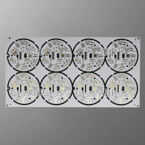
What are HDI PCBs Used?
The benefits explained above make these PCBs suitable for use in a number of applications, which include Medical Equipment, Industrial Control, Aerospace, consumer products and Military.
To know more about HDI PCBs, please contact us via [email protected].
| Item | Capability |
|---|---|
| Layers | 1-30 |
| Thicker Copper | 1-6OZ |
| Products Type | HF(High-Frequency)&(Radio Frequency) board, Impedance controlled board , HDI board ,
BGA& Fine Pitch board |
| Solder Mask | Nanya&Taiyo ;LPI & Matt Red, green, yellow,white, blue,black. |
| Base material | FR4(Shengyi China、ITEQ, KB A+,HZ), HI-TG, FR06, Rogers,Taconic、Argon and so on |
| Finished Surface | Conventional HASL,Lead-free HASL,Falsh Gold, ENIG (Immersion Gold)OSP(Entek), Immersion Tin,ImmersionSilver,Hard Gold |
| Selective Surface Treatment | ENIG(immersion Gold)+OSP, ENIG(immersion Gold)+Gold Finger,Flash Gold +Gold Finger,
immersion Silver+ Gold Finger, Immersion Tin+Gold Finger |
| Technical Specification | Minimum line width/gap:3.5/4mil(laser drill) Minimum hole size:0.15mm(mechanical drill)/4mil(laser drill) Minimum Annular Ring: 4mil Max Copper thickness: 6OZ Max Production size:900×1200mm Board Thickness:D/S: 0.2-7.0mm, Multilayers:0.40-7.0mm, Min Solder Mask Bridge:0.08mm Aspect ratio: 15:1 Plugging Visa capability: 0.2-0.8mm |
| Tolerance | Plated holes Tolerance:0.08mm(min±0.05) Non-plated hole tolerance:0.05min(min+0/-0.05mm or +0.05/-0mm) Outline Tolerance:0.15min(min±0.10mm) Functional test : Insulating resistance : 50 ohms (mormality) Peel off strength: 1.4N/mm Thermal Stress test :2650c,20 seconds Solder mask hardness:6H E-Test voltage :500V+15/-0V 30S Warp and Twist: 0.7% (semiconductor test board≤0.3% ) |