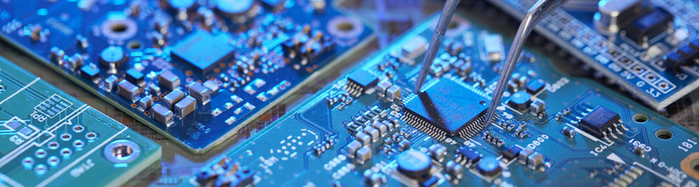
Printed circuit boards or PCBs are essential elements in the electronics world. They are used in more straightforward gadgets such as toys to complex devices such as military equipment.
Nevertheless, standard PCBs usually are used in low-power and low-voltage devices. This is to help them work properly. But what kind of PCB is used on devices that require more power and voltage? The answer is heavy copper PCB, in there, you will learn what heavy copper PCB is, the benefits of heavy copper PCB, the manufacturing process of heavy copper PCB, and much more.
What is heavy copper PCB?
A heavy copper PCB is a printed circuit board with a copper thickness of 3oz per sq. ft. But what makes a circuit board categorized as a heavy copper PCB is the thickness of its plating.
Copper thickness is improved by producing heavy copper PCB through plated holes and sidewalls. From example, if a PCB has two ounces of copper per sq. ft. thickness, that is a standard PCB.
But if the PCB has more than 3oz of copper, it is classified as heavy copper PCB. At the same time, a heavy copper PCB is different from an extreme copper PCB. An extreme copper PCB features 20oz to 200oz per sq. ft.
With the heavy copper PCB, the thickness helps the board conduct more current. The boards have more substantial mechanical power in the connector sites than the standard PCBs.
The benefits of heavy copper PCB
Heavy copper PCB comes with many benefits. Due to its unique features, it has become a perfect option for high-end applications. Here are the main benefits of heavy copper PCB.
1.Good thermal distribution
Due to their copper-plated vias, heavy copper PCBs provide good thermal distribution. Hence, they are used in applications that require high frequency and high speed. The PCB can be used in harsh temperatures.
2.Great mechanical strength
Another benefit of heavy copper PCB is its excellent mechanical strength. This makes it more durable and robust.
3.Excellent conductor
A heavy copper PCB is an excellent conductor. Hence, the PCB is used to make various electronics due to this benefit. It is possible to link several boards together, and they can quickly transfer current.
4.Have an excellent dissipation factor
Heavy copper PCBs are perfect for significant elements with a high loss of power. This is because they have an excellent dissipation factor. They prevent overheating form happening in electrical systems.
Difference between standard PCB and heavy copper PCB
Standard PCBs are quickly produced with copper etching and plating processes. The boards are plated to increase copper thickness to traces and planes. Also, the amount of copper used in standard PCBs is 1oz.
On the other hand, there are different manufacturing methods for heavy copper PCBs and the amount of copper used is more than 3oz.
With the standard printed circuit boards, cnc cutting, copper etching and plating methods are utilized. But heavy copper PCBs are obtained through various etching and step plating methods.
Standard PCBs perform lighter duties while heavy copper printed circuit boards perform heavy tasks. Also, the standard ones conduct a lower current while the heavy PCBs conduct a heavy current.
Applications of heavy copper PCB
Heavy copper PCBs come with numerous benefits over standard PCBs. In addition, they offer outstanding features making them perfect for specific applications.
For instance, heavy copper PCBs are ideal for defense and military applications, medical devices, and many other areas. Hence, the demand for heavy copper PCBs is continuously increasing.
Some of the applications of heavy copper PCBs are:
Solar power converters / Rail traction systems / Nuclear power industries / Automotive industries / UPS systems / Protective relays / Torque controls / Safety and signal systems / Welding equipment / Power line motors / Military equipment
| Item | Capability |
|---|---|
| Layers | 1-30 |
| Thicker Copper | 1-6OZ |
| Products Type | HF(High-Frequency)&(Radio Frequency) board, Impedance controlled board , HDI board ,
BGA& Fine Pitch board |
| Solder Mask | Nanya&Taiyo ;LPI & Matt Red, green, yellow,white, blue,black. |
| Base material | FR4(Shengyi China、ITEQ, KB A+,HZ), HI-TG, FR06, Rogers,Taconic、Argon and so on |
| Finished Surface | Conventional HASL,Lead-free HASL,Falsh Gold, ENIG (Immersion Gold)OSP(Entek), Immersion Tin,ImmersionSilver,Hard Gold |
| Selective Surface Treatment | ENIG(immersion Gold)+OSP, ENIG(immersion Gold)+Gold Finger,Flash Gold +Gold Finger,
immersion Silver+ Gold Finger, Immersion Tin+Gold Finger |
| Technical Specification | Minimum line width/gap:3.5/4mil(laser drill) Minimum hole size:0.15mm(mechanical drill)/4mil(laser drill) Minimum Annular Ring: 4mil Max Copper thickness: 6OZ Max Production size:900×1200mm Board Thickness:D/S: 0.2-7.0mm, Multilayers:0.40-7.0mm, Min Solder Mask Bridge:0.08mm Aspect ratio: 15:1 Plugging Visa capability: 0.2-0.8mm |
| Tolerance | Plated holes Tolerance:0.08mm(min±0.05) Non-plated hole tolerance:0.05min(min+0/-0.05mm or +0.05/-0mm) Outline Tolerance:0.15min(min±0.10mm) Functional test : Insulating resistance : 50 ohms (mormality) Peel off strength: 1.4N/mm Thermal Stress test :2650c,20 seconds Solder mask hardness:6H E-Test voltage :500V+15/-0V 30S Warp and Twist: 0.7% (semiconductor test board≤0.3% ) |