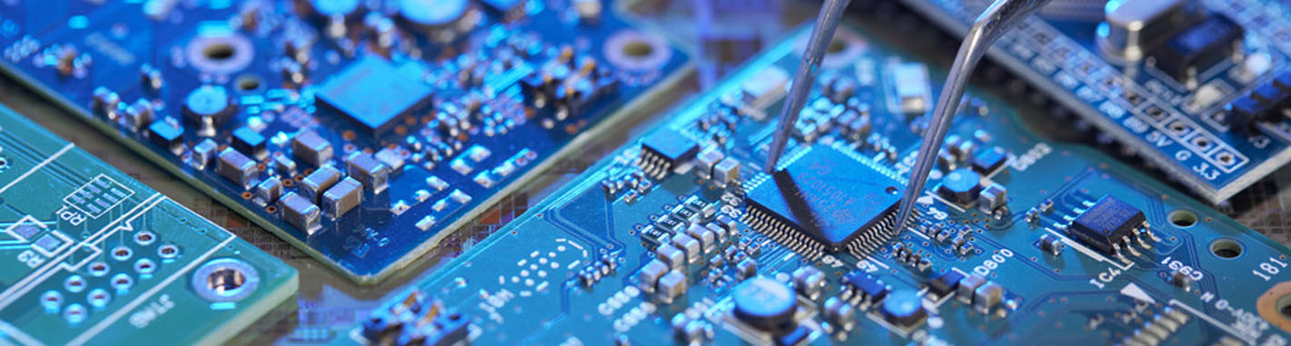
The increasing complexity of electronic components and switches continually requires faster signal flow rates, and thus higher transmission frequencies. Because of short pulse rise times in electronic components, it has also become necessary for high frequency (HF) technology to view conductor widths as an electronic component.
Depending on various parameters, HF signals are reflected on circuit board, meaning that the impedance (dynamic resistance) varies with respect to the sending component. To precent such capacitive effects, all parameters must be exactly specified, and implemented with the highest level of process control.
Critical for the impedances in high frequency PCBs are principally the conductor trace geometry, the layer buildup, and the dielectric constant of the materials used.
What is a high frequency PCB?
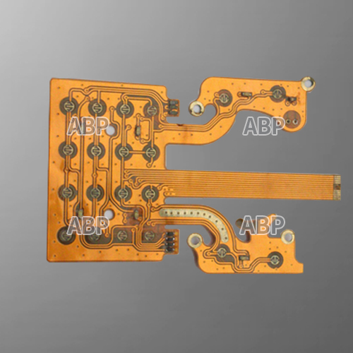
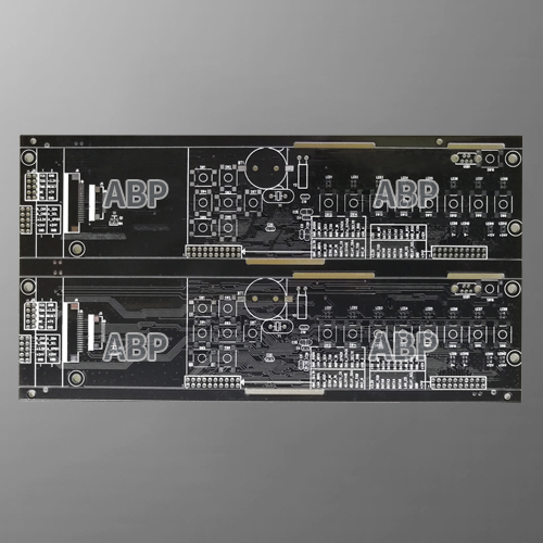
A high frequency printed circuit board, whether it’s rigid or flex, offers faster signal flow rates and a frequency range of up to 100 GHz. It’s important to note that there are numerous materials designed to operate at high frequency level. HF PCBs are defined by lower dielectric constant, lower dissipation factor, and low levels of thermal expansion. They are used regularly for HDI technology. They are also used extensively in high speed communications, telecommunications, and RF microwave technology.
Materials Used for HF PCBs
Special materials are required to achieve the high frequency provided by this type of PCB. There are a variety of substrate materials that will support your design and may differ based on signal speeds required and the application of the circuit board.
In terms of price, FR4 is the least expensive compared to dedicated high speed materials and Teflon,with Teflon being the most expensive. Though, FR-4 starts to drop off in performance when signal speed edges above 1.6 GHz.
Newer generation substrates, Teflon, and flex circuits are the best options when it comes to Dk, Df, water absorption, and survivability in the environment.
If a printed circuit board requires a frequency above 10GHz, newer generation substrates, Teflon, and Flex substrates are your best option since they are far superior to traditional FR-4 material.
The most common suppliers of high speed substrates are Rogers, Isola, Taconic, Dupont, and Megtron materials by Panasonic. All of these materials typically are lower Dk and lower loss.
Applications for HF PCBs
High frequency PCBs are used in many products and across many industries, including:
Cell phone / Telecommunications / Military and aerospace / RF microwave / Automotive / High-density interconnect and high-speed design applications
| Item | Capability |
|---|---|
| Layers | 1-30 |
| Thicker Copper | 1-6OZ |
| Products Type | HF(High-Frequency)&(Radio Frequency) board, Impedance controlled board , HDI board ,
BGA& Fine Pitch board |
| Solder Mask | Nanya&Taiyo ;LPI & Matt Red, green, yellow,white, blue,black. |
| Base material | FR4(Shengyi China、ITEQ, KB A+,HZ), HI-TG, FR06, Rogers,Taconic、Argon and so on |
| Finished Surface | Conventional HASL,Lead-free HASL,Falsh Gold, ENIG (Immersion Gold)OSP(Entek), Immersion Tin,ImmersionSilver,Hard Gold |
| Selective Surface Treatment | ENIG(immersion Gold)+OSP, ENIG(immersion Gold)+Gold Finger,Flash Gold +Gold Finger,
immersion Silver+ Gold Finger, Immersion Tin+Gold Finger |
| Technical Specification | Minimum line width/gap:3.5/4mil(laser drill) Minimum hole size:0.15mm(mechanical drill)/4mil(laser drill) Minimum Annular Ring: 4mil Max Copper thickness: 6OZ Max Production size:900×1200mm Board Thickness:D/S: 0.2-7.0mm, Multilayers:0.40-7.0mm, Min Solder Mask Bridge:0.08mm Aspect ratio: 15:1 Plugging Visa capability: 0.2-0.8mm |
| Tolerance | Plated holes Tolerance:0.08mm(min±0.05) Non-plated hole tolerance:0.05min(min+0/-0.05mm or +0.05/-0mm) Outline Tolerance:0.15min(min±0.10mm) Functional test : Insulating resistance : 50 ohms (mormality) Peel off strength: 1.4N/mm Thermal Stress test :2650c,20 seconds Solder mask hardness:6H E-Test voltage :500V+15/-0V 30S Warp and Twist: 0.7% (semiconductor test board≤0.3% ) |