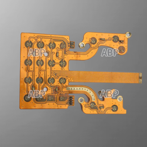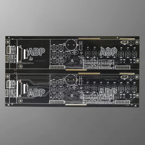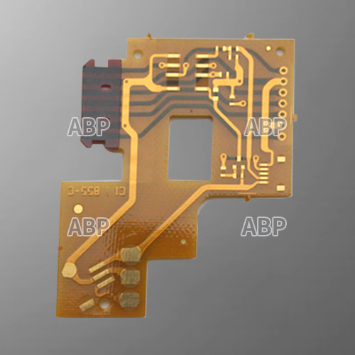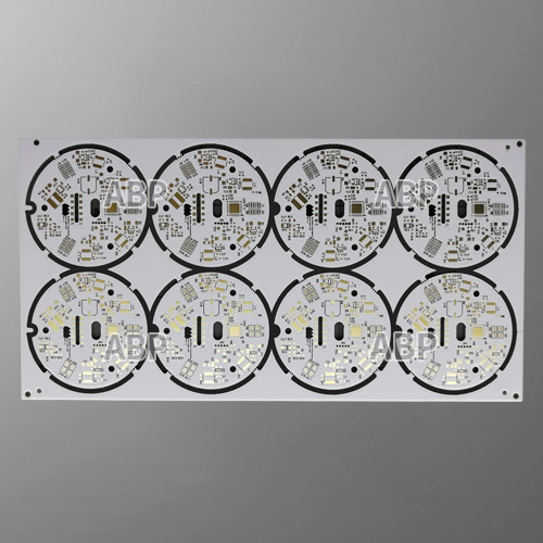
Multilayer PCB is a circuit board that has more than two layers. Unlike a double sided PCB which only has two conductive layers of material, all multilayer PCBs must have at least three layers of conductive material which are buried in the center of the material.
How are multilayer PCBs made?
Alternating layers of prepeg and core materials are laminated together under high temperature and pressure to produce multilayer PCBs. This process ensures that air isn’t trapped between layers, conductors are completely encapsulated by resin, and the adhesive that holds the layers together are properly melted and cured. The range of material combination is extensive from basic epoxy glass to exotic ceramic or Teflon materials.
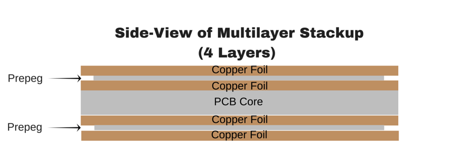
The figure above illustrates the stackup of a 4-Layer / multilayer PCB. Prepeg and core are essentially the same material, but prepeg is not fully cured, making it more malleable than the core. The alternating layers are then placed into a lamination press. Extremely high temperatures and pressures are applied to the stackup, causing the prepeg to “melt” and join the layers together. After cooling off, the end result is a very hard and solid multilayer board.
Benefits of multilayer PCBs
Compared to single or double sided PCBs, the benefits of multilayer PCBs are as follow:
Smaller – because multilayer PCBs combine multiple PCBs to create a more streamlined design with the same functionality.
Lighter – similar to the smaller aspect of multilayer PCBs with the combination of multiple boards you get a lighter product.
Durability – Multilayer PCBs are be durable by their nature as they are built to withstand their own heat and the weight.
Flexibility – some multilayer PCBs use flexible construction techniques, however this is not always the case. Find out more about Flexible PCBs.
Improved quality – a multilayer PCB is more complex than its single counterpart consequently more planning and work is put in and thy are often of better quality
Powerful: as extremely high-density assemblies multilayer boards are able to achieve greater capacity and speed despite their smaller size.
Applications of multilayer PCB
While the weight and space benefits of multilayer PCBs are especially valuable for aerospace PCBs, multilayer PCBs are also beneficial to applications where “cross-talk” levels are critical. These are a few other the applications using multilayer printed circuit boards: Computers / File Servers / Data storage / Signal transmission / GPS technology / Industrial controls / Satellite systems / Test equipment / X-ray equipment / Heart monitors / Atomic accelerators / Medical device / Communication equipment
| Item | Capability |
|---|---|
| Layers | 1-30 |
| Thicker Copper | 1-6OZ |
| Products Type | HF(High-Frequency)&(Radio Frequency) board, Impedance controlled board , HDI board ,
BGA& Fine Pitch board |
| Solder Mask | Nanya&Taiyo ;LPI & Matt Red, green, yellow,white, blue,black. |
| Base material | FR4(Shengyi China、ITEQ, KB A+,HZ), HI-TG, FR06, Rogers,Taconic、Argon and so on |
| Finished Surface | Conventional HASL,Lead-free HASL,Falsh Gold, ENIG (Immersion Gold)OSP(Entek), Immersion Tin,ImmersionSilver,Hard Gold |
| Selective Surface Treatment | ENIG(immersion Gold)+OSP, ENIG(immersion Gold)+Gold Finger,Flash Gold +Gold Finger,
immersion Silver+ Gold Finger, Immersion Tin+Gold Finger |
| Technical Specification | Minimum line width/gap:3.5/4mil(laser drill) Minimum hole size:0.15mm(mechanical drill)/4mil(laser drill) Minimum Annular Ring: 4mil Max Copper thickness: 6OZ Max Production size:900×1200mm Board Thickness:D/S: 0.2-7.0mm, Multilayers:0.40-7.0mm, Min Solder Mask Bridge:0.08mm Aspect ratio: 15:1 Plugging Visa capability: 0.2-0.8mm |
| Tolerance | Plated holes Tolerance:0.08mm(min±0.05) Non-plated hole tolerance:0.05min(min+0/-0.05mm or +0.05/-0mm) Outline Tolerance:0.15min(min±0.10mm) Functional test : Insulating resistance : 50 ohms (mormality) Peel off strength: 1.4N/mm Thermal Stress test :2650c,20 seconds Solder mask hardness:6H E-Test voltage :500V+15/-0V 30S Warp and Twist: 0.7% (semiconductor test board≤0.3% ) |