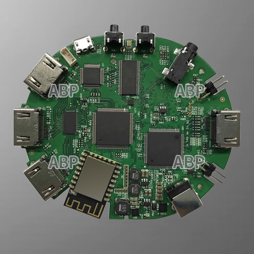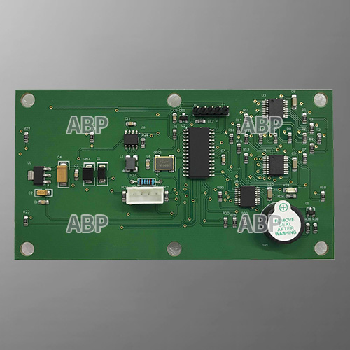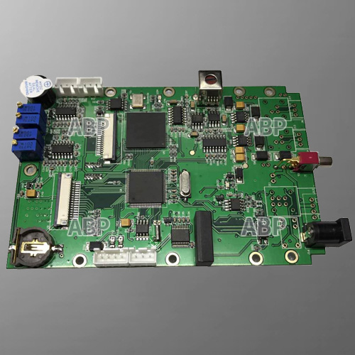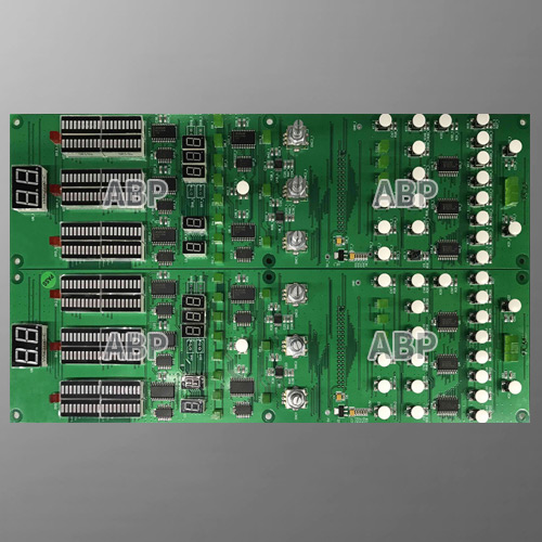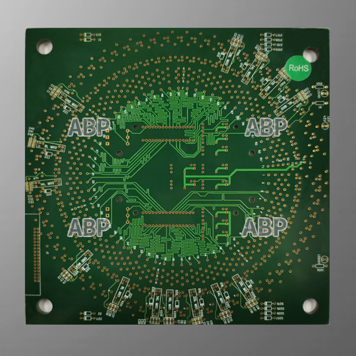
Multilayer PCB
Unlike a Double-Sided PCB which only has two conductive layers of material, all multilayer PCBs must have at least three layers of conductive material which are buried in the center of the material.
Benefits of Multilayer PCBs
Smaller size (considerable savings on space)
Increased flexibility.
Easier incorporation controlled impedance features.
EMI shielding through careful placement of power and ground layers.
Reduces the need for interconnection wiring harnesses (reduces overall weight)
| Item | Capability |
|---|---|
| Layers | 1-30 |
| Thicker Copper | 1-6OZ |
| Products Type | HF(High-Frequency)&(Radio Frequency) board, Impedance controlled board , HDI board ,
BGA& Fine Pitch board |
| Solder Mask | Nanya&Taiyo ;LPI & Matt Red, green, yellow,white, blue,black. |
| Base material | FR4(Shengyi China、ITEQ, KB A+,HZ), HI-TG, FR06, Rogers,Taconic、Argon and so on |
| Finished Surface | Conventional HASL,Lead-free HASL,Falsh Gold, ENIG (Immersion Gold)OSP(Entek), Immersion Tin,ImmersionSilver,Hard Gold |
| Selective Surface Treatment | ENIG(immersion Gold)+OSP, ENIG(immersion Gold)+Gold Finger,Flash Gold +Gold Finger,
immersion Silver+ Gold Finger, Immersion Tin+Gold Finger |
| Technical Specification | Minimum line width/gap:3.5/4mil(laser drill) Minimum hole size:0.15mm(mechanical drill)/4mil(laser drill) Minimum Annular Ring: 4mil Max Copper thickness: 6OZ Max Production size:900×1200mm Board Thickness:D/S: 0.2-7.0mm, Multilayers:0.40-7.0mm, Min Solder Mask Bridge:0.08mm Aspect ratio: 15:1 Plugging Visa capability: 0.2-0.8mm |
| Tolerance | Plated holes Tolerance:0.08mm(min±0.05) Non-plated hole tolerance:0.05min(min+0/-0.05mm or +0.05/-0mm) Outline Tolerance:0.15min(min±0.10mm) Functional test : Insulating resistance : 50 ohms (mormality) Peel off strength: 1.4N/mm Thermal Stress test :2650c,20 seconds Solder mask hardness:6H E-Test voltage :500V+15/-0V 30S Warp and Twist: 0.7% (semiconductor test board≤0.3% ) |