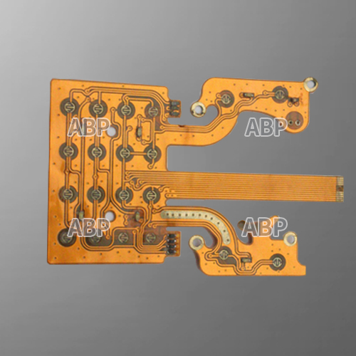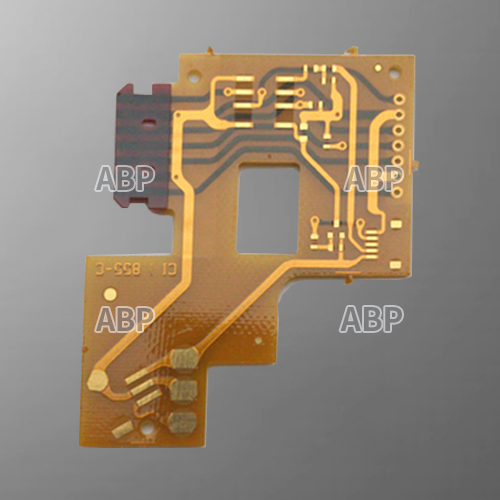
What is Rigid-flex PCB?
Rigid-flex PCB is a special flexible PCB composed of rigid PCB and flexible PCB laminated together, with a compact structure, and metalized holes to form electrical connections. It has the characteristics of high density, thin traces, small aperture, small size, light weight, and high reliability. It is still stable under vibration, impact, and humid environments.
Rigid-flex PCB has a bendable and three-dimensional installation, which effective use of installation space, is widely used in mobile phones, digital cameras, digital video cameras and other portable digital products.
Advantages of Rigid-flex PCB
Designing a rigid flex PCB is considerably more challenging than conventional rigid PCB. However, there are good reasons why rigid flex is used in some designs, particularly one that involves fitting the board in tight spaces.
Increase Reliability
Connectors serve their purpose when there’s a need to remove the wire harness from the PCB routinely. For a design that involves multiple interlinking subcircuits in an enclosure, adding connectors to the PCB only increases the risk of failure.
Space Saving
Often, the designs that call for a rigid flex PCB is one where space is luxury. For example, handheld thermal scanners can benefit from a rigid flex PCB design as there isn’t much space to fit in wire harnesses and high profile connectors. Instead, with the interconnecting circuit built-in on the flexible substrate, you’ll have more space to route the traces around.
Reduce Cost
Rigid flex PCBs are generally cheaper than their rigid counterparts, as the former is harder to produce. However, using rigid flex PCBs may reduce the overall cost of the product. As wired interconnects are replaced by the conductive layers of flexible material, you’ll save on the cost of assembly, which in some cases, involves manual labor.
As a rigid flex PCB is a complete circuit on its own, there isn’t a need for installing a wire harness in the enclosure it is mounted on. Such a wiring job takes up precious time and is an additional cost for each unit of the product.
Ease of Testing
It is also easy to automate testing of a rigid flex PCB as all the subcircuits are already interconnected when the PCB is manufactured. The ability to eliminate connectivity issues before the components are assembled, further, prevent unnecessary wastage and expense.
| Item | Capability |
|---|---|
| Layers | 1-30 |
| Thicker Copper | 1-6OZ |
| Products Type | HF(High-Frequency)&(Radio Frequency) board, Impedance controlled board , HDI board ,
BGA& Fine Pitch board |
| Solder Mask | Nanya&Taiyo ;LPI & Matt Red, green, yellow,white, blue,black. |
| Base material | FR4(Shengyi China、ITEQ, KB A+,HZ), HI-TG, FR06, Rogers,Taconic、Argon and so on |
| Finished Surface | Conventional HASL,Lead-free HASL,Falsh Gold, ENIG (Immersion Gold)OSP(Entek), Immersion Tin,ImmersionSilver,Hard Gold |
| Selective Surface Treatment | ENIG(immersion Gold)+OSP, ENIG(immersion Gold)+Gold Finger,Flash Gold +Gold Finger,
immersion Silver+ Gold Finger, Immersion Tin+Gold Finger |
| Technical Specification | Minimum line width/gap:3.5/4mil(laser drill) Minimum hole size:0.15mm(mechanical drill)/4mil(laser drill) Minimum Annular Ring: 4mil Max Copper thickness: 6OZ Max Production size:900×1200mm Board Thickness:D/S: 0.2-7.0mm, Multilayers:0.40-7.0mm, Min Solder Mask Bridge:0.08mm Aspect ratio: 15:1 Plugging Visa capability: 0.2-0.8mm |
| Tolerance | Plated holes Tolerance:0.08mm(min±0.05) Non-plated hole tolerance:0.05min(min+0/-0.05mm or +0.05/-0mm) Outline Tolerance:0.15min(min±0.10mm) Functional test : Insulating resistance : 50 ohms (mormality) Peel off strength: 1.4N/mm Thermal Stress test :2650c,20 seconds Solder mask hardness:6H E-Test voltage :500V+15/-0V 30S Warp and Twist: 0.7% (semiconductor test board≤0.3% ) |