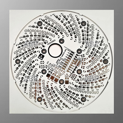
A Single Sided PCB is the most basic type of printed circuit board. It consists of only one conductive copper layer above the substrate. The electrical components are soldered or mounted on to one side of the board and the entire etched circuit can be seen on the other side of the board.
Single Sided Printed Circuit Boards are easy to design and manufacturing. They are also the most cost-effective PCBs.
Since these boards have only one conducting layer the conductive paths cannot cross or overlap and thus tend to take up a large amount of space. Due to this such PCBs are ideal for low-density design requirements.
Key features of Single-Sided PCB
-Low manufacturing and production cost
-Suitable for Low Density Designs
-Easy to manufacturing and design
-Easy to repair in case something goes wrong
Application of Single Sided PCB
Single sided PCBs are generally used in designs of low density and easy electronics. They can be designed and manufactured easily and quickly. Though single sided printed circuit boards are easy and simple, they are used by many electronic companies in the world in several electronic devices and gadgets: LED Lights / Calculator / Many sensors / Power supply / Timers / Radio / Printers / Camera
| Item | Capability |
|---|---|
| Layers | 1-30 |
| Thicker Copper | 1-6OZ |
| Products Type | HF(High-Frequency)&(Radio Frequency) board, Impedance controlled board , HDI board ,
BGA& Fine Pitch board |
| Solder Mask | Nanya&Taiyo ;LPI & Matt Red, green, yellow,white, blue,black. |
| Base material | FR4(Shengyi China、ITEQ, KB A+,HZ), HI-TG, FR06, Rogers,Taconic、Argon and so on |
| Finished Surface | Conventional HASL,Lead-free HASL,Falsh Gold, ENIG (Immersion Gold)OSP(Entek), Immersion Tin,ImmersionSilver,Hard Gold |
| Selective Surface Treatment | ENIG(immersion Gold)+OSP, ENIG(immersion Gold)+Gold Finger,Flash Gold +Gold Finger,
immersion Silver+ Gold Finger, Immersion Tin+Gold Finger |
| Technical Specification | Minimum line width/gap:3.5/4mil(laser drill) Minimum hole size:0.15mm(mechanical drill)/4mil(laser drill) Minimum Annular Ring: 4mil Max Copper thickness: 6OZ Max Production size:900×1200mm Board Thickness:D/S: 0.2-7.0mm, Multilayers:0.40-7.0mm, Min Solder Mask Bridge:0.08mm Aspect ratio: 15:1 Plugging Visa capability: 0.2-0.8mm |
| Tolerance | Plated holes Tolerance:0.08mm(min±0.05) Non-plated hole tolerance:0.05min(min+0/-0.05mm or +0.05/-0mm) Outline Tolerance:0.15min(min±0.10mm) Functional test : Insulating resistance : 50 ohms (mormality) Peel off strength: 1.4N/mm Thermal Stress test :2650c,20 seconds Solder mask hardness:6H E-Test voltage :500V+15/-0V 30S Warp and Twist: 0.7% (semiconductor test board≤0.3% ) |