
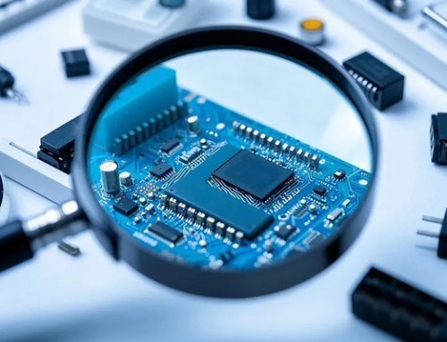
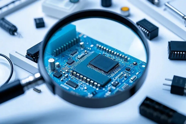
As electronics continue to shrink, PCB designers must pay more attention to where components are placed to ensure that every IC on a dense board “gets along.” With smaller boards, the risk for hot spots and thermal failure increases. Signal integrity also has to be taken into account with analog and digital circuits in close proximity. Creepage and clearance become trickier issues when there’s less real estate to put distance between chips. Last but not least, it is important to ensure that designs accurately convey the designer’s intent to the manufacturer to minimize manufacturing defects. The key to addressing many of these issues is SMT component placement. When every SMT component is in its right place, they’re all sure to get along a lot better.

PCB Thermal Considerations When Placing Components
High temperatures are one of the underlying causes of PCB failure. In a PCB with lots of real estate, thermal design is fairly straightforward. When it comes to a dense board, placing your SMT components to account for temperature becomes much more important.
Hotspots are something you always want to avoid on your PCB. In high-density PCBs, having too many power-hungry ICs near each other can cause these hotspots. Even passive parts like resistors can cause problems. If you must have a cluster of hot components close together, make sure you have a heat sink or use another method to evacuate that heat. SMT components aren’t always the problem; sometimes their traces are. High current traces can also produce heat, and if they’re all routed together, you may risk creating a hotspot. Therefore, you should try to keep high power chips and traces away from each other.
Sometimes, a high power chip may not look like a high power chip. Remember that some ICs have burst power modes where they can draw more current for a shorter period of time. This burst of power could create a temporary hotspot, especially if there are multiple chips doing it at the same time. Even short bursts of heat can be problematic. When temperatures oscillate between hotter and cooler in a PCB, they can degrade the materials that make up your board. The board substrate and solder have different CTEs, so when they heat up and cool down rapidly, they will expand differently. This can lead to cracked solder joints or break down dielectric material in your PCB. Be sure to carefully place SMT components on your board to avoid hotspots and thermal cycling.
Adequate Spacing and Signal Integrity Considerations
Now that you’ve gotten a refresher on thermal considerations, you’re ready to design your board, right? Not quite. Even more subtle signal integrity problems can arise when SMT components are placed carelessly. Not to mention you have to make sure there is enough space for ICs to begin with.
When placing your components, the first thing you should do is make sure they all have enough space. Usually, this means placing edge connectors first, as these may be dictated by the mechanical design. Next, watch out for high pin count components like BGAs. They may seem simple since all their connections are underneath the chip, but remember all of those pins have to be broken out to other parts of the board.
Now that everything has breathing room, it’s time to think about signal integrity. Remember that sensitive analog circuits don’t get along well with noisy digital components. Digital traces can act like transmitting antennas and analog traces like receiving ones. The larger a trace loop, the more it transmits or receives, so route traces carefully. Distance between circuits also helps reduce crosstalk, so try and keep analog and digital chips away from each other. You may still have to connect analog and digital parts or planes at a single point for grounding, which adds another piece to the puzzle. Last but not least, you should be aware that every plane or pad creates parasitic capacitance, and every long trace has some parasitic inductance. These can change the impedance of your perfectly balanced connections. You can hand-model these parasitic impedances or use design software to predict them.
SMT Component Placement Tips to Ensure Manufacturability
The final thing you’ll need to consider with SMT component placement is DFM and manufacturing defects. Follow these tips and work closely with your manufacturer to reduce problems during assembly.
When laying out your board panelization design, keep SMT components away from the edge. Large edge connectors can be especially problematic when using a router to depanelize your boards, so place your parts carefully.
It is a good design practice to orient similar components in the same direction. This is especially important if your board also includes through-hole components, which means that wave soldering will be necessary in addition to reflow for the SMTs.
Include reference indicators, like pin 1 location, to ensure components are oriented and connected properly.
Make sure that pad size matches the component package. Pad mismatch can adversely impact board assembly and performance once in operation.
Define your parts clearly in your designs and make sure that your design files accurately reflect your SMT component placement layout.
Choosing a nice place to live can be difficult, but sometimes choosing a spot for an SMT component can seem near impossible. These tips will help you place your SMT parts for optimal operation. Remember to consider the thermal impact of part placement and routing. Also, you’ll have to leave space for every IC and make sure chips aren’t transmitting or receiving too much noise.
