
With the growing complexity of electronics and the need for faster signal transmission rates, high-frequency PCBs are becoming an essential ingredient in developing high-performance applications across the manufacturing landscape.

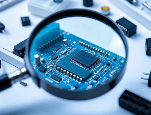
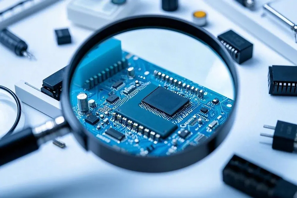
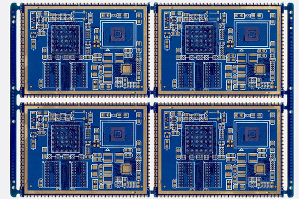
High-frequency printed circuit boards (PCBs) have emerged as the lifeline for electronics manufacturing. Such PCBs are known for their multiple features. Simply put, high-frequency PCBs transmit electromagnetic waves with minimal loss. And they ensure a high rate of signal flow. Some of the properties associated with high-frequency PCBs include:
-Low dissipation factor: The dissipation factor of high-frequency PCBs ranges between 0.0019 and 0.025. This ensures the signal transmission rate isn’t affected and that there’s minimal signal loss.
-Low dielectric constant: With a low and stable dielectric constant, there PCBs ensure smooth frequency transmission and minimal signal delay.
-Chemical resistance: The ability of high-frequency PCBs to withstand exposure to chemicals is of great value. It makes sure that the board doesn’t corrode and can be used in environments where there’s significant exposure to chemicals.
-Low moisture absorption: With a low rate of water absorption, these PCBs are fit to be used in damp and humid environments.
-Low dimensional stability: High-frequency PCBs are known to maintain their size and not be impacted by the environment’s temperature.
Due to these properties, their use is ubiquitous. However, PCB designers need to ensure that the following steps are carefully followed in designing high-frequency PCBs:
-Determine the PCB signal frequency: It’s important to ensure that the voltage and power demands are established. In addition, divide any power planes and figure out if different signals can be accommodated. It’s also important to ensure minimal tolerance levels as well as determine how to reduce noise levels.
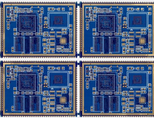
-Board stackup plan: The demands for the stackup layer must be planned put. The specific material and its constraints need to be understood.
-Floorplanning: You should divide the PCB into sections. In places that have digital and analog sections, proper isolation needs to be maintained to avoid interference.
-Power and ground planes: Once the PCB layout is defined, the next step is get a good grasp of the ground plan. Dividing the ground plane is imperative. You need to make sure that a resistor is included along with the signal trace to enhance the return path.
-Shrink the size of land patterns: High-frequency PCBs often have small pads. Reducing space helps minimize the parasitic capacitance and increases the mechanical strength.
-Route the frequency signals: High-frequency signals are known to produce high radiation. By routing the frequency signals effectively, you can prevent interference between signals.
-Use the 3W rule: Using the 3W rule ensures that signal integrity isn’t compromised. This rule establishes that there’s a difference between traces and the coupling effect is minimized.
-Apply the 20H rule: Coupling between ground and power planes can pose a threat to your design. With the 20H rule, you will ensure that the thickness between adjacent power and ground planes is more than the power plane.
Application of High-Frequency PCBs
High-frequency PCB usage is becoming more widespread. Some applications include:
-Communication systems in filtering devices, amplifiers, booster stations, and receivers.
-In the military for the production of ammunition and firearms.
-Radar systems that guide aircraft and avert accidents.
-Mission-critical diagnostic and monitoring devices in the medical industry.
Summary
High-frequency PCBs are vital for electronics PCB manufacturing. Their robust features make them the go-to device for electronic appliances. In particular, they play a major role in high-performance applications. With the growing complexity of electronics and the need for faster signal transmission rates, high-frequency PCBs will only increase in importance.