Services
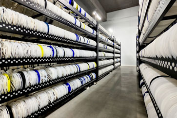
With 20 years’ experience in PCB fabrication, ABP have handled hundreds of thousands of PCB projects, and covered almost all kinds of substrate materials including FR4, Aluminum, Rogers, etc.
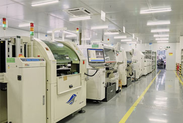
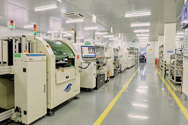
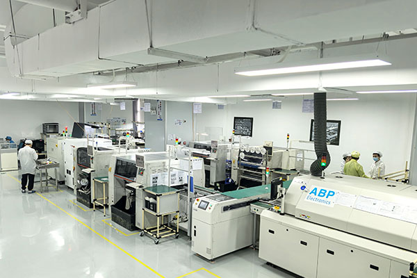
ABP has 2 major production bases in Shenzhen and Dongguan,with 5 smt production lines and 4 DIP production lines equipped with advanced testing instruments. Can provide customers with development and manufacturing services of diversified PCBA and finished products.
Component Sourcing
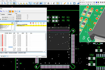
Design for Manufacturing or Design for Manufacturability (DFM) is the optimisation of a part, product, or component’s design, to create it cheaper and more easily. DFM involves efficiently designing or engineering an object, generally during the product design stage, when it is easier and less expensive to do so, to reduce manufacturing costs. This allows a manufacturer to identify and prevent mistakes or discrepancies.
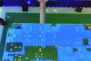
As a professional PCB board coating provider, our factory is equipped with a professional production line, including two sets of conformal coating spraying equipment, UV inspection, baking and other automatic equipment. If your PCBA board has the requirements of temperature and humidity, durability, insulation, waterproof and dustproof, then you need the service of circuit board coating,please contact us.
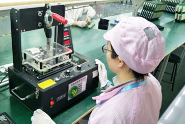
PCBA test refers to the detection of electrical continuity and input and output values of PCBA. In the design of PCB boards, there are numerical relationships between different test points, such as voltage and current. To verify whether the PCB board meets the design requirements, it is necessary to use professional test equipment to test points. PCBA test is a key to ensure the quality of production and delivery.
Visit our online factory
To help you quickly learn about our services and production capabilities, we have launched an online factory. Please click the link below to visit our online factory.
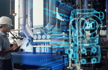
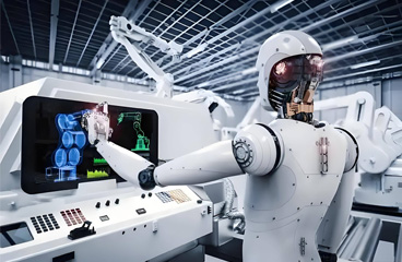
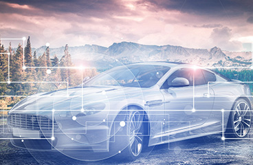
OUR INDUSTRY
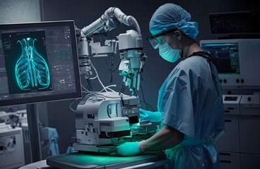
ABP has cooperated with 2000 customers in fields of industrial control, communications, medical electronics, computers and peripherals, semiconductors, automotive electronics, etc., in more than 70 countries and regions throughout the world.