
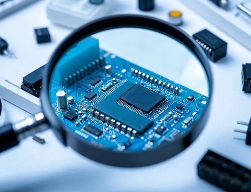
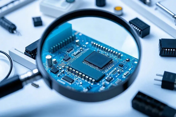
A PCB assembly process requires collective and sustained attention to ensure the end product’s quality. In the absence of a solid PCB assembly defect detection system, you may miss a tilted component or a bad solder web despite rigorous manual testing. If you are lucky, it may only cost you some additional reworks. Worst case scenario: You just lost an entire project. Let’s have a look at some common PCB defects, understand their impact on end-product quality, and learn how to avoid them altogether with a failure-proof testing strategy in place.
Common PCB Defects and Their Impact on Product Quality
Solder Bridges
Defined as a defect under IPC-A-610D, a solder bridge is formed when two-component pads on a PCB that are not designed to be electrically connected become joined together due to the application of excess solder, even a small bridge can create a conduction path between components and lead to a short circuit or component burn up. Early detection of print defects directly after the print operation and before component placement enables board manufacturers to save time on defective board assembly and costly reworks.
Tombstoning
Also known as the Manhattan or crocodile effect, Tombstoning refers to a partial or complete lifting of passive SMT components during the PCB reflow soldering process. It can occur due to different wetting speeds, improperly designed solder pads, PCB contamination, or improper pad size. The tombstoning phenomenon directly affects the quality and reliability of PCBs while leading to extra repair costs if they are not detected in time.
Position Shifts
Sometimes, displacement of components on a wet solder paste may occur in the SMT of pick-and-place (P&P) machines. Such small position shifts are often underestimated and assumed to be taken care of during the reflow soldering process. The component shift may occur due to poor quality solder paste application, excess flux-flow during reflow, improper handing of components after the P&P process, or insufficient air pressure from the nozzle. Once a component shifts its position, it will affect the board’s overall performance and reliability.
Solder Webbing
Boards occasionally include a web-like combination of solder and flux residues. These solder residues are referred to as solder webbing, Webbing can occur due to a number of reasons, including solder contamination, extensive mask pollution, or faulty curing of resins on the board. It adversely affects the solder joint’s quality, leading to unreliable signal transfer and tombstoning.
Blowholes
Blowholes, or pinholes, are associated with the release of moisture from the through-hole board via thin copper plating or voids during wave soldering. Excess moisture, flux, or poor drilling of bare boards with gaps between the platting and the laminate can give rise to blowholes. Initially, the holes may be confined to specific locations, but progressively spread throughout the entire board.
Problems with a Traditional Troubleshooting Strategy
Not having an automated PCB assembly defect detection system in place requires a significant amount of manual work. A more traditional PCB troubleshooting strategy typically includes a number of tiresome steps. First, you have to perform a visual inspection to trace simple problems like solder bridges, tombstoning, and footprint mismatches. If the boards pass the first step, it’s time to check for any possible assembly defect or faulty components. If nothing works, removing the components from the board and testing them against required functionalities should be your last step; however, if the component is very small or comes with dense pins, you will find it hard to re-solder it back to the board.
The process can be tedious and time-consuming, which increase the probability of human error, design flaws, reworks, and lead time.
Using an Automated PCB Assembly Defect Detection System To Improve Product Quality
When your PCB assembly defect detection system includes highly reliable, feature-heavy, and automated robots, there is hardly any room for errors.
Solder Paste Inspection (SPI)
A 3D solder paste inspection machine is valuable element of the PCB assembly process. It checks for solder paste deposits-including their shape, volume, and coverage-and provides immediate feedback through a graphic interface. An early detection system helps manufacturers avoid material wastage, extra expenditure, and excessive downtime owing to unwanted revisions.
Automated Optical Inspection (AOI)
Automated optical inspection (AOI) equipment is specially designed to test PCBs for effective quality control during the assembly process. It closely looks for any defect by making use of several light sources and high-definition cameras. Common PCB defects such as open circuits, solder bridges, solder shorts, lifted leads, and missing components can be easily identified with an AOI machine in the assembly line.
Digitally Controlled Reflow
SMD reflow ovens run on extremely uniform temperature profiles digitally programmed and controlled for enhanced process control. It enables maximum heat transfer at the lowest Delta T temperature, further minimizing power consumption. Advanced ovens with an inert nitrogen atmosphere replace oxygen to avoid surface oxidation and widen the process window. Nitrogen also improves the visual appearance of he board surface by making them smoother and shinier. As the reflow process is digitally optimized, manufacturers tend to a lot of setbacks such as poor solder joints, damaged components, and cols soldering.
X-ray Inspection
An image processing technique like X-ray inspection appropriately isolates paste from non-paste regions and can help you with bridge detection. The “paste-only” 3D view enables you to easily inspect exposed pad-solder joints underneath the IC from any angle. It can comfortably inspect all types of components (SMD, BGA, LGA, QFN) and their solder joints through a program. The inspection effectiveness rate is very high despite the short inspection time. Moreover, it finds deep faults below a BGA component that are hard to notice with the naked eyes.
Flying Probe Test
The flying probe test (FPT) is a program-based PCB testing tool that instructs flying probes to make contact with a unit’s vias and test pads to check for defects. It is capable of checking for any shorts, opens, or component values. As the system makes use of a high-resolution camera, finding a missing component is easy. It calls for a short overall test time, generates quick feedback, and offers high conversion flexibility.
