
Even if you’ve never fabricated a PCB, you might be familiar with the process. PCB etching involves the application of UV-resistant laminate to a presensitized photoresist copper layer, which is then exposed to UV rays. Areas that are not covered will be etched off in a special etching solution.
The PCB minimum etch technique has more to do with what happens at the design stage than the process of PCB etching itself. It refers to the idea of keeping as much copper area on the PCB as possible. Effectively, what minimum etch does is impose a tradeoff – it improves heat dissipation, while making parasitic capacitance more prominent.
When you’re working on a double-sided PCB, you often have ground planes on the top and bottom surfaces. However, it’s unlikely that ground copper exists on each part of the layer. Sections of copper that are not connected to the ground are removed during etching.
PCB minimum etch technique ensures a uniform ground plane
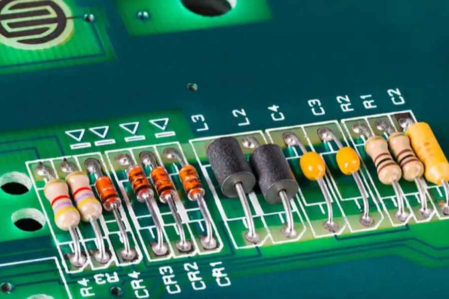
You can see in the image how small areas between the traces on the PCB are not covered by ground-connected copper.
If the PCB minimum etch technique is employed, there wouldn’t be pockets of copperless areas on the PCB. The surface of the PCB would be uniformly covered by copper pour, which is connected to the ground.
What’s the Purpose of PCB Minimum Etch Technique?
If you are not sure of the answer to this question, just know that PCB minimum, etch technique is an unfamiliar term even to some experienced designers. However, there is a legitimated reason to employ PCB minimum etch technique in certain scenarios. The grounded copper plane is known for its shielding effect and that’s what makes it a useful strategy in mitigating on-board interference.
If you’re designing a mixed-signal PCB, the rule of thumb is to keep analog and digital signals apart. Failure to do so will risk digital noise coupling into adjacent traces. Yet, you don’t always have the luxury of more space on a PCB. In such circumstances, PCB minimum etching is a handy design consideration.
By having more copper on the surface of the PCB, you won’t be leaving sensitive traces unguarded. The copper acts like a shield that protects analog signals from being compromised by digital noise. It also ensures that you have a better-filled ground plane that acts as the return path to adjacent signals.
