
In PCB design, engineers must navigate numerous challenges to ensure their products’ long-term reliability and functionality. One such challenge is managing strain and flexure in printed circuit boards. Here will explore the common causes of PCB strain and flexure, discuss the impact of depanelizing, and provide actionable tips for design engineers to minimized these issues and improve the overall performance of their designs.
Common Causes of PCB Strain and Flexure
1. Component Placement and Orientation
The placement and orientation of components on a PCB can significantly impact strain and flexure. Heavy or large footprint components can cause uneven stress distribution, resulting in potential board flexure or warping.
2. Board Materials and Thickness
The choice of the board materials and thickness plays a crucial role in determining the rigidity and flexibility of the PCB. Thinner boards may be more prone to flexure and strain, leading to potential reliability issues.
Mechanical Stress during Assembly and Depanelizing
PCBs are subjected to various forms of mechanical stress during the assembly process, such as soldering, component placement, and depanelizing. These stresses can cause strain and flexure, leading to potential long-term reliability concerns.
3. PCB Depanelization
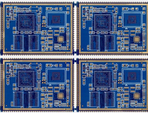
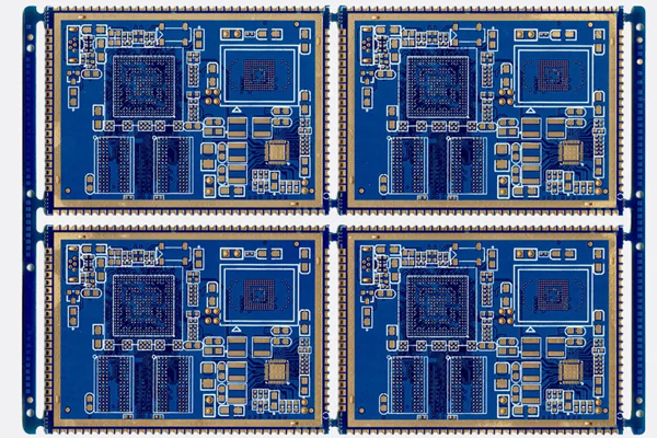
After completing the PCB assembly process, depanelizing separates individual PCBs from a large panel. This process can introduce mechanical stress, causing board strain and flexure. The method used for depanelizing, such as routing, V-scoring, or laser cutting, can also affect the amount of stress imparted on the PCB.
Actionable Tips to Minimize PCB Strain and Flexure Issues
To minimize PCB strain and flexure issues, design engineers can employ the following best practices:
1. Optimize Component Placement
Carefully consider component placement and orientation to evenly distribute mass and minimize strain on the PCB. Consider supporting large or heavy components, such as a mechanical standoff or additional solder on through-hole components.
2. Choose Appropriate Board Materials and Thickness
Selecting the suitable board material and thickness minimizes flexure and strain. Consult your PCB manufacturer to determine the best materials and thickness for your design requirements.
3. Implement Proper Routing Techniques
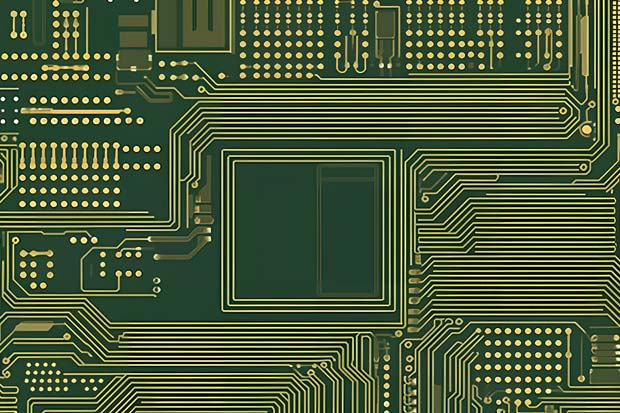
Design your PCB layout with proper routing techniques to minimize stress concentrations and reduce the risk of flexure or warping. This includes avoiding right-angle traces, using curved or chamfered corners, and ensuring adequate trace spacing.
4. Use Fiducial Marks
Fiducial marks help assembly machines accurately align components, reducing mechanical stress during component placement. Incorporate fiducial marks in your PCB design to improve assembly accuracy and reduce the risk of strain and flexure.
5. Select the Right Depanelizing Method
Choose the appropriate depanelizing method based on your PCB design and material properties that minimize mechanical stress and potential strain or flexure issues.

