
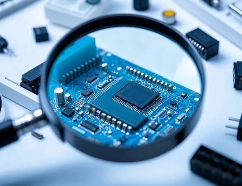
When it comes to PCB design, power routing is a critical aspect that can significantly impact the functionality and performance of a circuit board. Poor power routing can lead to various issues such as voltage drops, noise, and even damage to the components. Therefore, it is essential to follow some best practices and techniques to ensure an efficient and reliable power distribution network. In this article, we will discuss a few essential techniques for PCB power routing.

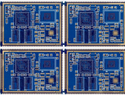
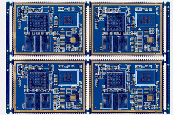
Plan your power routes: Before starting the actual routing, it is crucial to plan your power routes carefully. Identify the high-current paths and critical components that require stable power supply. Ensure that the power routes are as short as possible to minimize voltage drops and reduce resistance. It is also important to separate the power and ground planes to prevent crosstalk and interference.
Use the right tools and software: Utilize advanced PCB design tools and software that offer powerful routing features. These tools provide realistic simulations and help you visualize the power distribution network. They can also help in identifying potential issues and allowing you to make necessary adjustments before manufacturing the PCB.
Employ appropriate trace widths and spacing: The width and spacing of the power traces play a crucial role in determining the efficiency of power distribution. Ensure that the trace width is sufficient to carry the maximum expected current without exceeding the temperature rise limits. Additionally, maintain adequate spacing between the power traces and other components to prevent overheating and ensure proper cooling.
Minimize power plane transitions: Power plane transitions can introduce unnecessary impedance and voltage drops. Try to minimize the number of transitions by using continuous power planes whenever possible. If a transition is unavoidable, use a wide trace or a via to ensure a smooth transition and minimize the impact on the overall power distribution network.
Consider the use of decoupling capacitors: Decoupling capacitors are essential for maintaining a stable power supply and reducing voltage fluctuations. Place decoupling capacitors close to the power pins of critical components to ensure a quick response to voltage changes. It is also important to choose the appropriate capacitance value and ensure that the decoupling capacitors are correctly oriented.
Address potential noise sources: Identify and mitigate potential noise sources in the power distribution network. This includes ensuring proper grounding, using ferrite beads or inductors to filter high-frequency noise, and avoiding tight spacing between power traces and high-speed signals.
Test and validate your design: Once the PCB design is complete, it is essential to test and validate the power distribution network. Perform power integrity analysis and simulate the actual operating conditions to identify any potential issues. This can help you make necessary adjustments and ensure that your PCB operates efficiently and reliably.
In conclusion, PCB power routing is a critical aspect of PCB design that requires careful planning, attention to detail, and the use of appropriate techniques and tools. By following the tips mentioned above, you can create an efficient and reliable power distribution network, resulting in a better-performing PCB.
