
In the layout of printed circuit boards, width plays an important part, especially in the metal connections fabricated into the board called “traces”. Traces conduct signals to and from the pins of the components soldered to the board and carry varying amounts of current depending on the net. Additionally, the signal’s traces may have special electrical needs affecting their size, and trace widths must be carefully controlled for error-free manufacturing. This article will look at these different variables as we answer the question, what is trace width in PCB layout?
The Importance of Trace Widths for Correct PCB Fabrication and Assembly
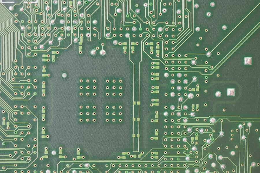
Traces are metal connections of various widths between solder pads usually fabricated from copper during the circuit board etching process. Although the etching will change based on which board layer is being fabricated, the desired copper weight (thickness), and the type of materials used to build the board, the basic process is as follows:
-Photoresist materials are applied to the copper-covered core material used to build the circuit board
-The traces, pads, and other PCB circuitry elements are exposed onto the photoresist causing those areas to harden into a protective coating
-The remaining photoresist is chemically removed, but the hardened photoresist remains over those areas that will become the copper circuitry of the board layer
-The copper layer is then etched to remove the unprotected copper leaving only the traces and other copper circuitry on the layer
-Once the protective photoresist is removed chemically, the board layer is composited with other layers to build up the circuit board
Etching by nature is an aggressive process. Fabricators need to exercise great caution to ensure that the traced are not over-etched, resulting in the traces being fabricated to less than their desired widths. Also, traces isolated on the board may etch down more than traces clustered together in groups due to the concentration of etching on that one area. Sometimes it pays so slightly widen isolated traces to guard against them etching smaller than desired. You could seriously degrade the signal integrity of the board with traces that are over-etched and don’t meet their target widths. Another important aspect of PCB fabrication is the thickness, or “weight”, of the copper being etched. Traces with a greater copper weight can not be etched down as much as other traces due to their thickness.
Trace widths can also impact the soldering processes used during circuit board assembly. Wide traces used in power and ground routing can act like a heat sink leading to uneven soldering temperatures and poor solder joints. When this happens to large parts, such as high pin-count BGAs or surface mount connectors, the imperfections can be difficult to find and correct, requiring expensive inspection rework techniques. But as complex as the manufacturing problems associated with incorrect trace widths are, they can an even larger effect on the electrical performance of the board, which we will look at next.
Circuit Requirements and Understanding What is Trace Width in PCB Layout
When it comes to the electrical performance of the board, trace widths play an essential part in both signal and power integrity.
Signal integrity
Different trace widths are often used to improve signal integrity to control crosstalk, electromagnetic interference (EMI), and other problems associated with signal interference. Here are some examples:
Controlled impedance routing: While most digital traces are routed with the minimum trace width, certain high-speed signals need to be routed at specific widths to control their impedance. If the length of these lines has different impedance values scattered through them, the impedance values scattered through them, the impedance mismatches can create reflections of the signal and disrupt its performance. To prevent this problem, the trace widths of these lines must be precisely determined based on calculations of the dielectric material of the board, spacing to other signals, and the copper weight being used.
Microstrip and stripline: Sensitive high-speed transmission lines need to be closely coupled with a reference ground plane for shielding their traces. An internal routing layer sandwiched between two ground planes is known as a stripline configuration, while traces on the board’s exterior with only the adjacent plane beneath it is a microstrip configuration. The stripline traces will be narrower due to the use of double-ground planes to match the impedance of the lines between the two configurations.
Analog routing: Analog signals should be as short and direct as possible and wider than other routing. This extra width helps keep impedance low. It is also better to minimize the use of vias with routing analog circuitry and keep the traces on the same layer.
Power integrity
Differing trace widths are also needed to ensure clean power delivery to the components on the circuit board. Here are some areas to keep an eye on during layout:
Short and direct routing: Just as with analog routing, you will want to keep your traces as short as possible to reduce the chance of these traces behaving like antennas and creating additional noise. It is also helpful to use 45° or rounded corners when possible instead of right angles.
Use wide traces: Using wider traces with power routing will help reduce inductance in the line and crosstalk.
Current and thermal considerations: Power traces conduct different current levels depending on which net is being routed. Therefore, prepare to use different trace widths and copper weights as necessary. The amount of heat these lines generate with their current also needs to be considered; the more current, the more heat. Additionally, the power traces on the external layers of the board can benefit from air-cooling, but internal power routing cannot. Therefore, internal power traces need to be wider than their counterparts on the surface layers.

