
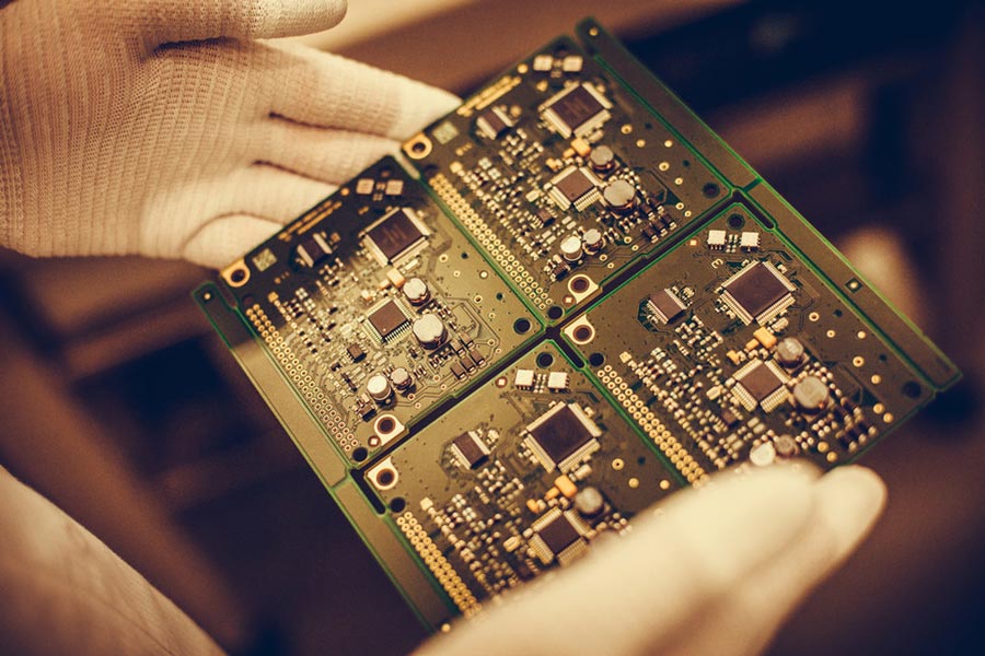
Multilayer printed circuit boards (PCBs) have become an integral part of modern electronic devices, offering increased functionality and reduced size. The complexity of multilayer PCB assembly lies in the design, which must be optimized for manufacturability to ensure high-quality and reliable products. This article explores the key considerations and best practices for designing multilayer PCBs that can be efficiently assembled.
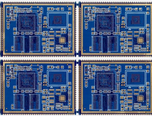
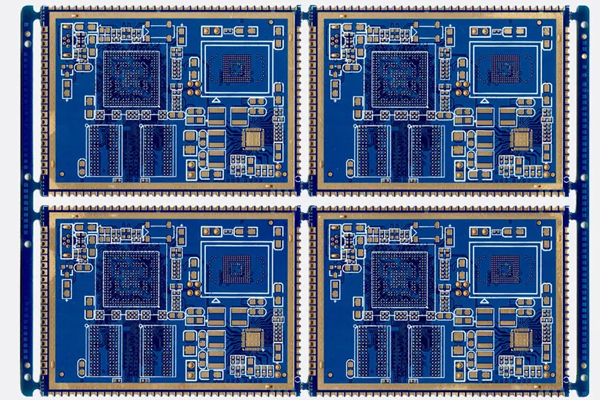
Board Layout and Stackup: The layout and stackup of a multilayer PCB are critical factors that impact manufacturability. Careful planning of the board’s layers, signal routing, and power planes is essential to minimize manufacturing defects. Designers should follow established guidelines for stackup construction, considering the required dielectric constant and signal integrity. Additionally, the use of standard board sizes can facilitate automated assembly processes.
Component Placement: Efficient component placement is crucial for streamlining the assembly process. Designers should prioritize the placement of high-frequency components and sensitive components away from noise sources. Components with similar footprints should be grouped together to facilitate automated placement and reduce setup time. Additionally, minimizing the distance between components and the board edges can aid in achieving optimal yields during assembly.
Signal Routing: Proper signal routing is essential for maintaining electrical performance and reducing manufacturing risks. Designers should employ controlled impedance routing techniques to ensure signal integrity, especially for high-speed signals. Avoiding sharp corners and vias in critical signal paths can reduce crosstalk and signal loss. Moreover, using standard via sizes and types can simplify the assembly process and improve quality.
Power Distribution Network (PDN) Design: A well-designed power distribution network is crucial for reliable multilayer PCB operation. Designers should focus on minimizing power loop inductance and resistance to reduce voltage drops and ensure stable power delivery. Employing decoupling capacitors and bulk capacitance strategically can improve PDN performance. Additionally, separating power and ground planes can aid in simplifying the assembly process and enhancing product reliability.
Manufacturing Constraints and Tolerances: Designers must consider manufacturing constraints and tolerances when designing multilayer PCBs. Adhering to standard design rules, such as minimum trace widths and spacing, can facilitate the assembly process and minimize errors. Moreover, designers should account for assembly tolerances, such as component placement accuracy and board flatness, to ensure proper fit and functionality.
Design for Testability (DFT): Designing multilayer PCBs with testability in mind is crucial for quality assurance and troubleshooting. Designers should incorporate test points, such as probing pads and built-in test features, to facilitate electrical testing during assembly and post-assembly. Additionally, following established DFT guidelines can aid in reducing manufacturing defects and improving overall product reliability.
Design for Assembly (DFA): Designing multilayer PCBs with assembly efficiency in mind can significantly impact manufacturing costs and time-to-market. Designers should optimize board thickness, component lead lengths, and PCB stiffness to facilitate automated assembly processes. Additionally, employing right-angle components and minimizing the use of fine-pitch components can simplify assembly and reduce assembly time.
Designing for manufacturability in multilayer PCB assembly is a complex process that requires careful planning and consideration of various factors. By following best practices for board layout, component placement, signal routing, power distribution, manufacturing constraints, and design for testability and assembly, designers can create multilayer PCBs that are efficient to manufacture, assemble, and maintain. Ultimately, optimizing the design for manufacturability can lead to higher product quality, reduced manufacturing costs, and shorter time-to-market.

